Showing 81–96 of 249 results
-
£219.99
Graphene Transferred onto SiO₂ Substrate (1 cm x 2 cm) CAS Number: 7782-42-5 Substrate Size: 1 cm x 2 cm Preparation Method: Graphene film is grown on copper foils via Chemical Vapor Deposition (CVD) and transferred onto SiO₂/Si substrates with a 300 nm SiO₂ layer using a PMMA (polymethyl methacrylate) layer and wet chemical transfer…
-
£289.99
Graphene Transferred onto SiO₂ Substrate (2 cm x 2 cm) CAS Number: 7782-42-5 Substrate Size: 2 cm x 2 cm Preparation Method: Graphene film is grown on copper foils via Chemical Vapor Deposition (CVD) and transferred onto SiO₂/Si substrates with a 300 nm SiO₂ layer using a PMMA (polymethyl methacrylate) layer and wet chemical transfer…
-
£319.99
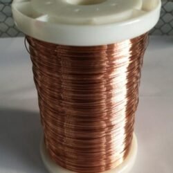
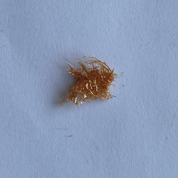
Graphene-Coated Copper Wire (Per Meter) CAS Number: 7782-42-5 Product Dimensions: Available in custom lengths; price listed per meter. Preparation Method: Graphene is grown on copper wire using a Chemical Vapor Deposition (CVD) process. The uniform graphene coating enhances the wire’s conductivity and surface properties. Morphology Options: Continuous Graphene Coating For specific customization requirements regarding coating…
-
£899.99
Hexagonal Boron Nitride (h-BN) Grown on Copper Foil (10 cm x 10 cm) CAS Number: 10043-11-5 Preparation Method: Hexagonal boron nitride (h-BN) films are grown on copper foils using a Chemical Vapor Deposition (CVD) process, resulting in high-quality and uniform layers. Morphology Options: Monolayer Few Layers (<10 layers, ~5 nm) Multilayer (>5 nm) All options…
-
£699.99
Hexagonal Boron Nitride (h-BN) Grown on Copper Foil (5 cm x 10 cm) CAS Number: 10043-11-5 Preparation Method: Hexagonal boron nitride (h-BN) films are grown on copper foils using a Chemical Vapor Deposition (CVD) process, resulting in high-quality and uniform layers. Morphology Options: Monolayer Few Layers (<10 layers, ~5 nm) Multilayer (>5 nm) All options…
-
£499.99
Hexagonal Boron Nitride (h-BN) Grown on Copper Foil (5 cm x 5 cm) CAS Number: 10043-11-5 Preparation Method: Hexagonal boron nitride (h-BN) films are grown on copper foils using a Chemical Vapor Deposition (CVD) process, resulting in high-quality and uniform layers. Morphology Options: Monolayer Few Layers (<10 layers, ~5 nm) Multilayer (>5 nm) All options…
-
£219.99
Hexagonal Boron Nitride (h-BN) Transferred onto PET Substrate (1 cm x 1 cm) CAS Number: 10043-11-5 Preparation Method: Hexagonal boron nitride (h-BN) films are first grown on copper foils using a high-temperature Chemical Vapor Deposition (CVD) process. These high-quality h-BN films are then carefully transferred onto flexible PET (polyethylene terephthalate) substrates using a PMMA-assisted wet…
-
£219.99
Hexagonal Boron Nitride (h-BN) Transferred onto Quartz Substrate (1 cm x 1 cm) CAS Number: 10043-11-5 Preparation Method: Hexagonal boron nitride (h-BN) films are initially grown on copper foils using a high-temperature Chemical Vapor Deposition (CVD) process. These high-quality h-BN films are then transferred onto quartz substrates using a PMMA-assisted wet chemical transfer technique to…
-
£219.99
Hexagonal Boron Nitride (h-BN) Transferred onto Sapphire Substrate (1 cm x 1 cm) CAS Number: 10043-11-5 Preparation Method: Hexagonal boron nitride (h-BN) films are grown on copper foils using a high-temperature Chemical Vapor Deposition (CVD) process. These high-quality h-BN films are then carefully transferred onto sapphire substrates using a PMMA-assisted wet chemical transfer technique, ensuring…
-
£219.99
Hexagonal Boron Nitride (h-BN) Transferred onto SiO₂ Substrate (1 cm x 1 cm) CAS Number: 10043-11-5 Preparation Method: Hexagonal boron nitride (h-BN) films are first grown on copper foils via a high-temperature Chemical Vapor Deposition (CVD) process. These high-quality h-BN films are subsequently transferred onto SiO₂/Si substrates (300 nm SiO₂ layer) using a PMMA-assisted wet…
-
£499.99 – £999.99Price range: £499.99 through £999.99
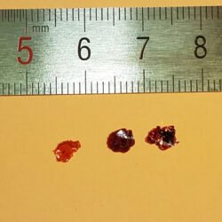
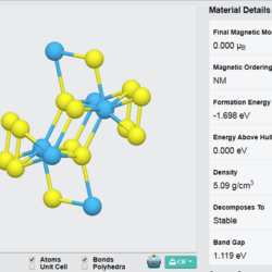
HfS₂ Crystals HfS₂ is a layered transition metal dichalcogenide (TMD) with a van der Waals structure, known for its notable electronic, optical, and catalytic properties. As an indirect bandgap semiconductor, it exhibits excellent carrier mobility, strong optical absorption, and environmental stability, making it a promising material for nanoelectronics, optoelectronics, and energy storage applications. Our HfS₂…
-
£499.99 – £569.99Price range: £499.99 through £569.99
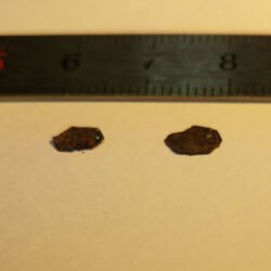
HfS₃ Crystals HfS₃ is a layered transition metal trichalcogenide (TMT) with a quasi-one-dimensional (1D) structure. It exhibits unique anisotropic electronic and optical properties, making it a promising material for optoelectronics, 2D material studies, and energy storage applications. Our HfS₃ crystals are synthesized using the Chemical Vapor Transport (CVT) method, ensuring high purity, precise stoichiometry, and…
-
£499.99 – £999.99Price range: £499.99 through £999.99
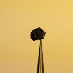
HfSe₂ Crystals HfSe₂ is a layered transition metal dichalcogenide (TMD) with a van der Waals structure, known for its strong electronic, optical, and catalytic properties. As an indirect bandgap semiconductor, HfSe₂ exhibits excellent carrier mobility, strong optical absorption, and high environmental stability, making it a promising material for applications in nanoelectronics, optoelectronics, and energy storage….
-
£499.99 – £1,199.99Price range: £499.99 through £1,199.99
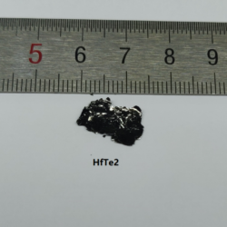
HfTe₂ Crystals HfTe₂ is a layered transition metal dichalcogenide (TMDC) with a van der Waals structure, exhibiting semimetallic behavior, strong spin-orbit coupling, and excellent environmental stability. It is a promising material for quantum research, optoelectronic devices, and energy-related applications. Sample Size Options: Crystals larger than 10 mm² Crystals larger than 25 mm² Crystals larger than…
-
£499.99 – £999.99Price range: £499.99 through £999.99
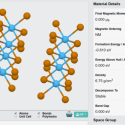
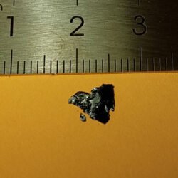
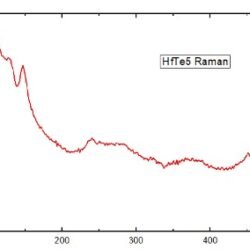
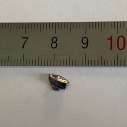
HfTe₅ Crystals HfTe₅ is a layered transition metal pentatelluride with strong electronic, optical, and thermal properties. Known for its quasi-two-dimensional structure, HfTe₅ exhibits unique quantum transport phenomena, such as the chiral anomaly, and is a promising material for quantum materials research, thermoelectric applications, and optoelectronic devices. Sample Size Options: Crystals larger than 10 mm² Crystals…
-
£499.99 – £569.99Price range: £499.99 through £569.99
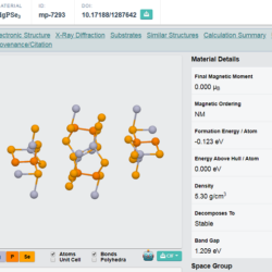
HgPSe₃ Crystals HgPSe₃ is a layered van der Waals material belonging to the family of transition metal thiophosphates. It exhibits unique semiconducting and optical properties, making it a promising material for optoelectronics, energy storage, and 2D materials research. Our HgPSe₃ crystals are synthesized using the Chemical Vapor Transport (CVT) method to ensure high purity, precise…