-
£599.99
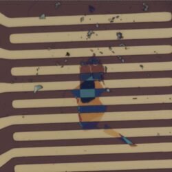
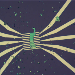
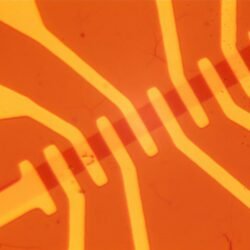
Black Phosphorus/ReSe₂ FET Device Heterojunction FET Device Device Structure: Conductive Si Substrate / 300 nm SiO₂ Layer / 5 µm Gold Electrode Array / ReSe₂ / Black Phosphorus Device Description & Features: 2D van der Waals Heterojunction: The combination of anisotropic black phosphorus (BP) and ReSe₂ forms a type-II band-aligned heterostructure, enabling efficient charge separation…
-
£599.99
Graphene FET Device Device Structure: Conductive Si Substrate / 300 nm SiO₂ Layer / Graphene Channel / Cr+Au Electrodes Device Description & Features: High-Performance 2D Material: Graphene is a single-layer honeycomb lattice of carbon atoms, offering ultrahigh carrier mobility, linear band dispersion, and tunable electronic properties. Back-Gated FET Configuration: The SiO₂/Si back-gate structure provides effective…
-
£599.99
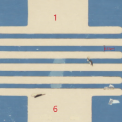
Mechanically Exfoliated Black Phosphorus FET Device Black Phosphorus (BP) FET Device Device Structure: Highly Doped Conductive Si Substrate / 300 nm SiO₂ Layer / Au Electrodes / Mechanically Exfoliated Few-Layer Black Phosphorus Device Specifications: Channel Width: 5 µm Few-Layer Black Phosphorus (BP) For specific thickness requirements, please contact us. Device Description & Features: High-Mobility 2D…
-
£599.99
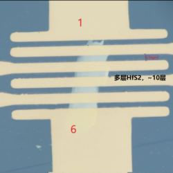
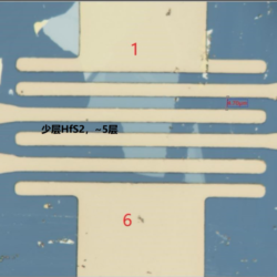
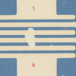
Mechanically Exfoliated HfS₂ FET Device Device Structure: Au Electrodes / HfS₂ / 300 nm SiO₂ / Si Back-Gated FET HfS₂ Layer Options: Few-layer (~5 layers) Multilayer (~10 layers) For specific thickness requirements, please contact us. Device Description & Features: High-Mobility 2D Semiconductor: Hafnium disulfide (HfS₂) is a layered transition metal dichalcogenide (TMD) with high electron…
-
£599.99
Mechanically Exfoliated Monolayer Graphene FET Device Structure: Highly Doped Conductive Si Substrate / 300 nm SiO₂ Layer / Monolayer Graphene / Cr+Au Electrodes Device Specifications: Graphene Thickness: Monolayer Electrode Material: Cr+Au Gate Dielectric: 300 nm SiO₂ For specific device modifications, please contact us. Device Description & Features: Ultra-High Carrier Mobility: Graphene exhibits ballistic transport, extremely…
-
£599.99
Mechanically Exfoliated ReS₂ FET Device ReS₂ FET (Back-Gated ReS₂ FET) Device Structure: Au Electrodes / ReS₂ / 300 nm SiO₂ / Si Back-Gated FET Device Specifications: Channel Width: 5 µm Few-layer (~5 layers) Multilayer (~10 layers) For specific thickness requirements, please contact us. Device Description & Features: Anisotropic 2D Semiconductor: Rhenium disulfide (ReS₂) is a…
-
£599.99
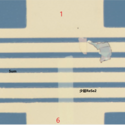
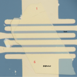
Mechanically Exfoliated ReSe₂ FET Device ReSe₂ FET (Back-Gated ReSe₂ FET) Device Structure: Au Electrodes / ReSe₂ / 300 nm SiO₂ / Si Back-Gated FET ReSe₂ Layer Options: Few-layer (~5 layers) Multilayer (~10 layers) For specific thickness requirements, please contact us. Device Description & Features: Anisotropic 2D Semiconductor: Rhenium diselenide (ReSe₂) is a layered transition metal…
-
£599.99
Mechanically Exfoliated WS₂ FET Device WS₂ FET (Back-Gated WS₂ FET) Device Structure: Au Electrodes / WS₂ / 300 nm SiO₂ / Si Back-Gated FET WS₂ Layer Options: Monolayer Few-layer ( ~5 layers) Multilayer (~10 layers) For specific thickness requirements, please contact us. Device Description & Features: High-Performance 2D Semiconductor: Tungsten disulfide (WS₂) is a layered…
-
£599.99
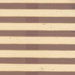
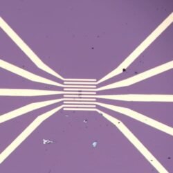
Monolayer 2H-MoTe₂ FET Device Device Structure: Conductive Si Substrate / 300 nm SiO₂ Layer / 5 µm Gold Electrode Array / Monolayer 2H-MoTe₂ Device Description & Features: High-Performance 2D Semiconductor: Molybdenum ditelluride (MoTe₂) in its 2H phase is a layered transition metal dichalcogenide (TMD) with a direct bandgap (~1.1 eV in monolayer form), making it…
-
£599.99
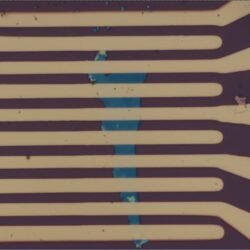
MoS₂ FET Device Device Structure: Conductive Si Substrate / 300 nm SiO₂ Layer / Few-layer or Multilayer MoS₂ / Au+Cr+Au Electrodes MoS₂ Layer Options: Few-layer (~5 layers) or Multilayer (~10 layers) Custom Layer Thickness Available – Please Contact Us Device Description & Features: High-Performance 2D Semiconductor: Molybdenum disulfide (MoS₂) is a layered transition metal dichalcogenide…
-
£599.99
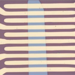
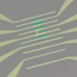
Multilayer ReS₂/PdSe₂ FET Device Device Structure: Conductive Si Substrate / 285 nm SiO₂ / Au Electrodes / Exfoliated Multilayer PdSe₂ / Exfoliated Multilayer ReS₂ Material Specifications: Multilayer PdSe₂ Multilayer ReS₂ For specific thickness requirements, please contact us. Device Description & Features: Heterostructure 2D FET: The combination of PdSe₂ and ReS₂ forms a unique type-II van…
-
£599.99
WS₂ FET Device Device Specifications: Packaging: Single device (1 unit per package) Device Dimensions: 1 cm x 1 cm Substrate: SiO₂/Si (Silicon with 300 nm SiO₂ layer) Device Structure: SiO₂/Si Substrate / WS₂ Channel / Au or Cr+Au Electrodes Device Description & Features: High-Performance 2D Semiconductor: Tungsten disulfide (WS₂) is a layered transition metal dichalcogenide…
-
£599.99
WSe₂ FET Device Device Specifications: Packaging: Single device (1 unit per package) Device Dimensions: 1 cm x 1 cm Substrate: SiO₂/Si (Silicon with 300 nm SiO₂ layer) Device Structure: SiO₂/Si Substrate / WSe₂ Channel / Au or Cr+Au Electrodes Device Description & Features: High-Performance 2D Semiconductor: Tungsten diselenide (WSe₂) is a layered transition metal dichalcogenide…