GeS Crystals
Price range: £499.99 through £549.99
Dispatch normally within 1 business day; carrier transit normally 6–8 business days (7–9 business days in total). See Shipping Policy and Returns Policy.
For research and laboratory use only. Not for medical, diagnostic or household use.
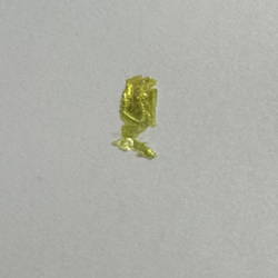
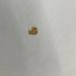
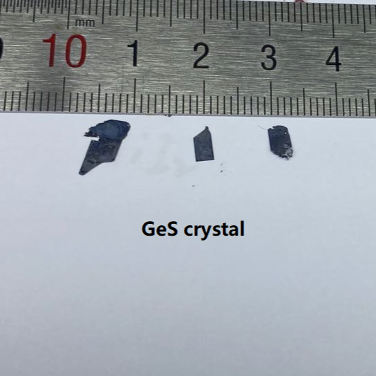
GeS Crystals
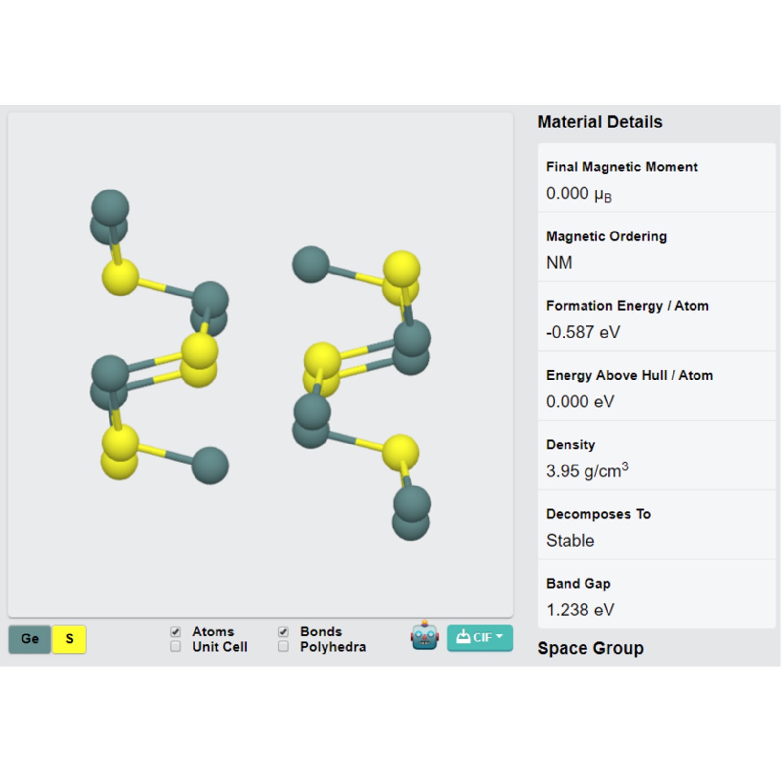
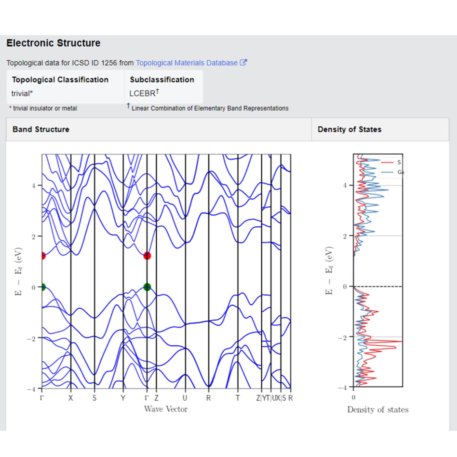
GeS is a layered semiconductor material belonging to the family of group-IV monochalcogenides. It exhibits strong anisotropic optical and electronic properties due to its unique orthorhombic crystal structure. With a narrow bandgap and high environmental stability, GeS is a promising material for optoelectronics, photovoltaics, and 2D material research.
Sample Size Options:
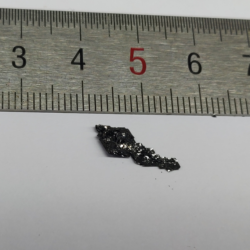
Crystals larger than 10 mm²
Crystals larger than 25 mm²
Material Properties:
Layered Structure: Applicable for exfoliation into thin layers for 2D applications.
Anisotropic Properties: Exhibits strong direction-dependent optical and electronic behavior. Narrow Bandgap: (~1.6 eV), applicable to visible to near-infrared applications. Thermal and Chemical Stability: Maintains performance under controlled conditions.
Crystal Structure:
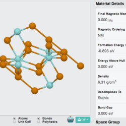
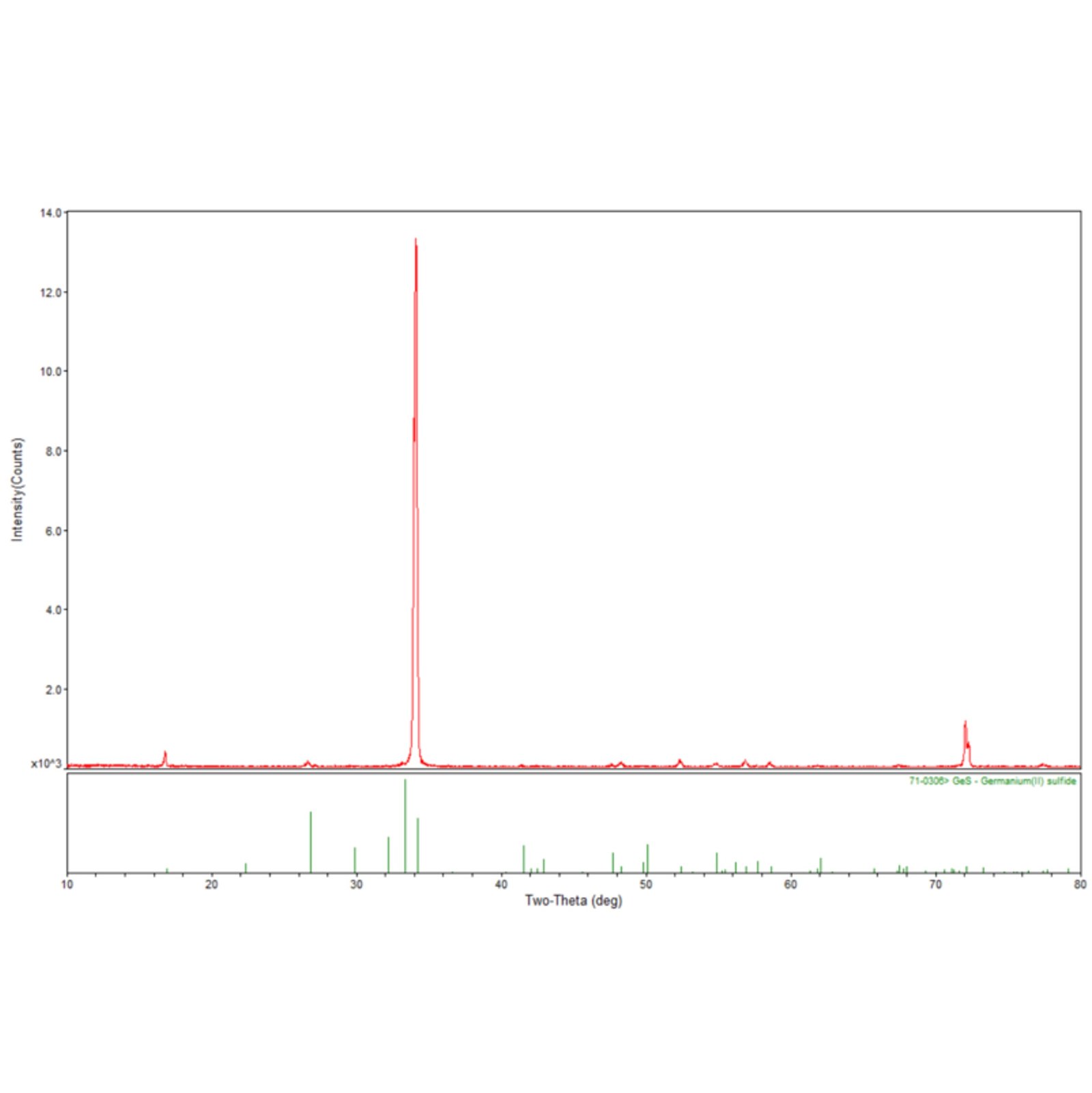
Type: Orthorhombic layered structure
Features: Easily cleavable into thin sheets, applicable to nanoscale studies.
Degree of Exfoliation:
Ease of Use: Readily exfoliates into monolayers or few-layer sheets for specialized research.
Other Characteristics:
Optoelectronic Properties: High quantum efficiency and strong light absorption for photonic devices.
Photovoltaic Potential: Applicable to solar energy conversion applications.
Environmental Stability: Consistent under inert conditions, with long-term usability.
Applications:
Optoelectronics:
Applicable for photodetectors, LEDs, and light-sensitive devices. Photovoltaics:
Promising for solar cells due to its narrow bandgap and optical properties.
2D Material Research:
Applicable for exfoliation into thin layers for van der Waals heterostructures. Sensors:
High sensitivity to light and chemical stimuli, making it applicable for specialized sensing applications. Quantum Materials Research:
Permits exploration of low-dimensional electronic and optical phenomena.
References:
1, Madatov, R., A. Alekperov, and O. Hasanov. “Effect of Nd Impurity on Photoconductivity and Optical Absorption Spectra of GeS Single Crystal.” Journal of Applied Spectroscopy 84.1 (2017).
2,Madatov, R., A. Alekperov, and O. Hasanov. “Effect of Nd Impurity on Photoconductivity and Optical Absorption Spectra of GeS Single Crystal.” Journal of Applied Spectroscopy 84.1 (2017).
3,Zhang, Shengli, et al. “Two-dimensional GeS with variable electronic properties via external electric field and strain.” Nanotechnology 27.27 (2016): 274001.
Specifications
| Material | GeS Crystals |
|---|---|
| Chemical formula | GeS |
| Crystal structure | Orthorhombic layered structure |
| Available sizes | Crystals larger than 10 mm²; Crystals larger than 25 mm² |
Typical properties of the bulk material (literature values)
| Space group | Pnma (No. 62), COD 1010649 |
|---|
Source: Crystallography Open Database (COD); the entry ID is given with each value. Reference values for the bulk substance, not test results of a specific lot.
| Option 1 | > 10 mm², > 25 mm² |
|---|