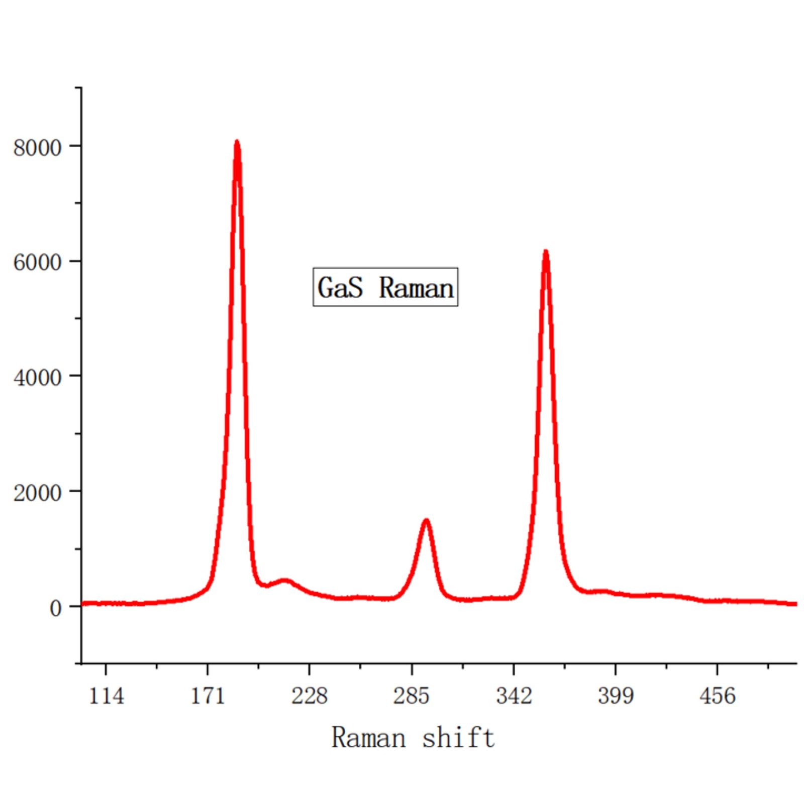
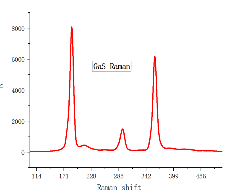
GaS Crystals
Price range: £499.99 through £569.99
Dispatch normally within 1 business day; carrier transit normally 6–8 business days (7–9 business days in total). See Shipping Policy and Returns Policy.
For research and laboratory use only. Not for medical, diagnostic or household use.
GaS Crystals
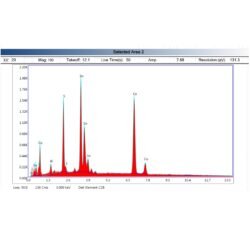
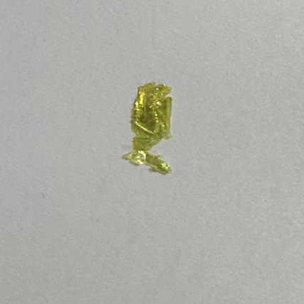
GaS is a layered semiconductor belonging to the group-III metal chalcogenides, with a van der Waals structure that makes it applicable for 2D material research. GaS exhibits a wide bandgap and high photoconductivity, making it applicable to optoelectronic devices, energy applications, and nanoscale electronics. Our GaS crystals are grown using high-temperature vapor transport techniques to with high purity, structural quality, and consistent physical properties.
Sample Size Options:
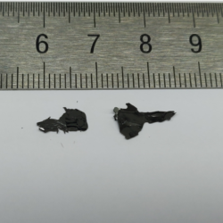
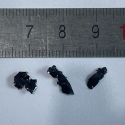
Crystals larger than 10 mm²
Crystals larger than 25 mm²
Material Properties:
Layered van der Waals Structure: Facilitates exfoliation into thin layers for 2D research. Wide Bandgap: (~2.5 eV), applicable to UV and visible light optoelectronics.
High Photoconductivity: Strong light absorption and carrier mobility.
Environmental behavior: Maintains performance under inert storage conditions.
Crystal Structure:
Type: Layered monoclinic structure
Features: Easily cleavable, permits the formation of thin films and 2D layers.
Degree of Exfoliation:
Ease of Use: Readily exfoliated into thin layers for specialized 2D material applications.
Other Characteristics:
Optoelectronic Properties: High quantum efficiency in UV and visible ranges.
Semiconducting Nature: Promising for nanoscale electronic and photonic devices.
Chemical behavior: Highly consistent in controlled inert environments, with durability for research and applications.
Applications:
Optoelectronics:
Applicable for photodetectors, light-emitting diodes, and other devices operating in the UV and visible ranges.
2D Material Studies:
High for exfoliation into thin layers and exploring heterostructures with other van der Waals materials. Quantum Materials Research:
Permits investigations into the electronic and optical behavior of 2D semiconductors. Energy
Applications:
Applicable to solar cells, photocatalysis, and other energy conversion technologies. Sensors:
High sensitivity to light and chemical stimuli, making it applicable for optical and chemical sensing devices.
Typical properties of the bulk material (literature values)
| Chemical formula | GaS |
|---|---|
| CAS number | 12024-10-1 |
| Molar mass | 101.79 g/mol |
Sources: PubChem (U.S. National Library of Medicine) and NIST (National Institute of Standards and Technology). Reference values for the bulk substance, not test results of a specific lot.
| Option 1 | > 10 mm², > 25 mm² |
|---|