
Bi₂S₃ Crystals
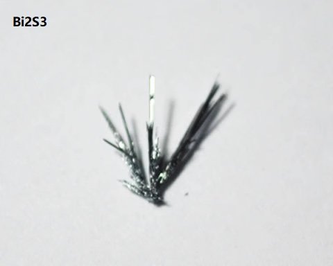
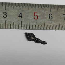
Bi₂S₃ (Bismuth Sulfide) is a layered semiconductor material known for its excellent thermoelectric, optoelectronic, and photocatalytic properties. It has a narrow bandgap and high absorption coefficient, making it highly suitable for applications in photodetectors, thermoelectric devices, and solar energy conversion. Our Bi₂S₃ crystals are synthesized using the Chemical Vapor Transport (CVT) method, ensuring high purity, superior crystallinity, and uniform structural properties.
Sample Size Options:
Crystals larger than 10 mm²
Crystals larger than 25 mm²
Crystals larger than 100 mm²
Material Properties:
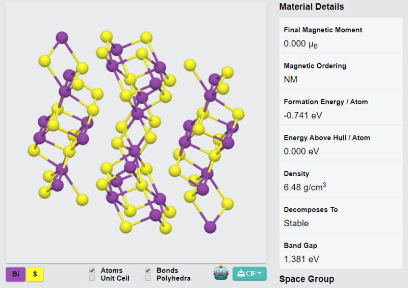
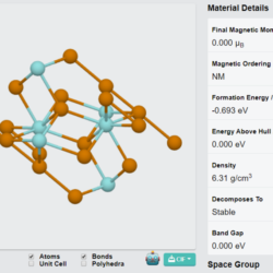
Layered Orthorhombic Structure: Facilitates easy exfoliation into thin layers for 2D material research.
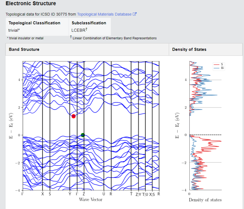
Narrow Bandgap: Bandgap of ~1.3 eV, suitable for infrared detectors and photovoltaic applications.
High Absorption Coefficient: Strong light absorption in the visible and near-infrared regions, ideal for photodetectors and solar cells.
Thermoelectric Performance: Promising material for thermoelectric applications due to its high Seebeck coefficient.
Environmental Stability: Stable under ambient conditions, making it suitable for long-term applications.
Crystal Structure:
Type: Orthorhombic layered structure
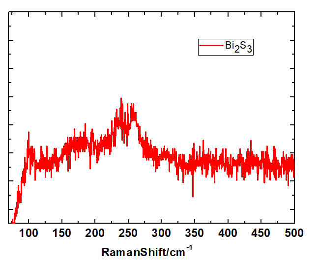
Features: High crystallinity with uniform, defect-free layers, ideal for thin-film fabrication and nanoscale device applications.
Degree of Exfoliation:
Ease of Use: Can be exfoliated into thin layers for advanced materials research and device fabrication.
Other Characteristics:
Photocatalytic Activity: Effective for photocatalytic applications, including water splitting and pollutant degradation.
Anisotropic Transport Properties: Exhibits direction-dependent electrical and thermal conductivity, suitable for advanced device designs. Eco-Friendly Composition: Composed of non-toxic and earth-abundant elements, making it environmentally friendly for large-scale applications.
Applications:
Optoelectronics:
Ideal for photodetectors, infrared sensors, and photovoltaic devices due to strong light absorption. Thermoelectric Devices:
High thermoelectric performance for energy conversion and waste heat recovery applications. Energy Storage:
Potential applications in batteries and supercapacitors due to its layered structure. Photocatalysis:
Suitable for photocatalytic hydrogen production and environmental remediation.
2D Material Studies:
Can be exfoliated into thin layers for use in van der Waals heterostructures and 2D materials research. Synthesis Method:
Chemical Vapor Transport (CVT): Ensures high-quality crystals with excellent purity, uniform thickness, and high structural integrity.
| Option 1 | > 10 mm², > 100 mm², > 25 mm² |
|---|
Related products
-
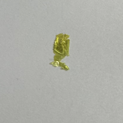
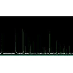
GaS Crystals
Price range: £499.99 through £569.99 -
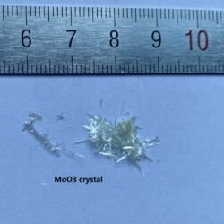
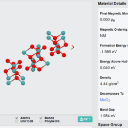
α-MoO₃ Crystals
Price range: £459.99 through £499.99 -
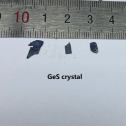
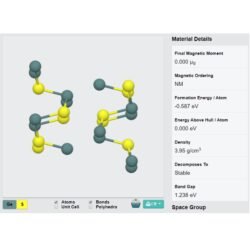
GeS Crystals
Price range: £499.99 through £549.99 -
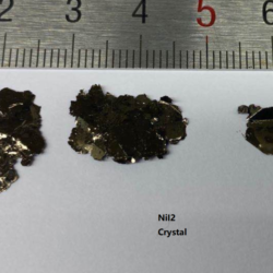
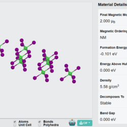
NiI₂ Crystals
Price range: £499.99 through £998.99 -
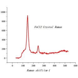
FeCl₂ Crystals
Price range: £499.99 through £569.99 -

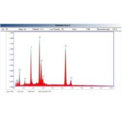
Co₃Sn₂S₂ Crystals
£599.99 -
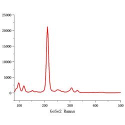
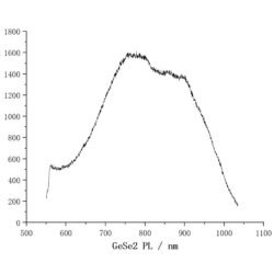
GeSe₂ Crystals
Price range: £499.99 through £569.99 -
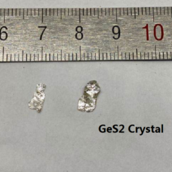
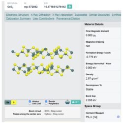
GeS₂ Crystals
Price range: £499.99 through £599.99 -

MoTe₂ Crystals (2H phase)
Price range: £499.99 through £569.99 -
ZrTe₃ Crystals
Price range: £499.99 through £599.99