
Bi₂Se₃ Crystals
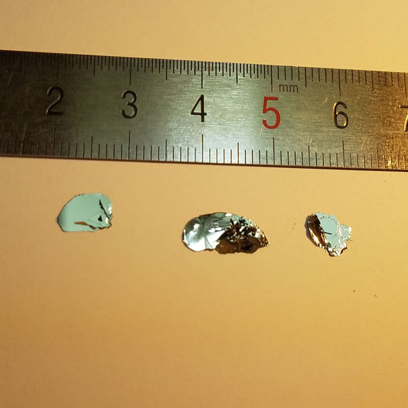
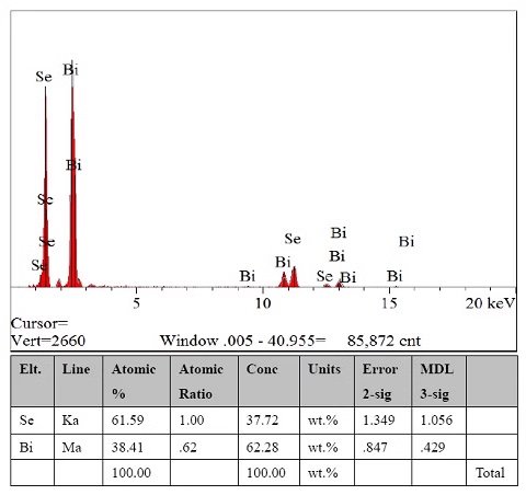
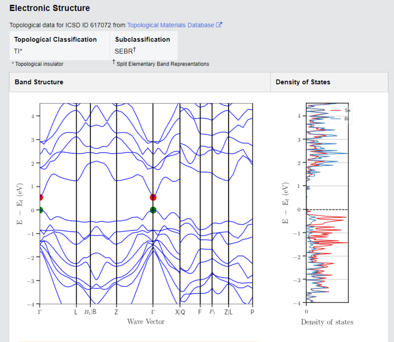
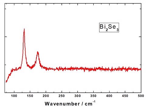
Bi₂Se₃ (Bismuth Selenide) is a layered topological insulator with a rhombohedral crystal structure. It exhibits strong spin-orbit coupling, making it an ideal candidate for quantum computing, spintronics, and thermoelectric applications. Bi₂Se₃ is also widely used in optoelectronics, nanoelectronics, and energy storage devices. Our Bi₂Se₃ crystals are synthesized using the Chemical Vapor Transport (CVT) method, ensuring high purity, well-controlled stoichiometry, and good crystallinity.
Sample Size Options:
Crystals larger than 10 mm²
Crystals larger than 25 mm²
Crystals larger than 100 mm²
Material Properties:
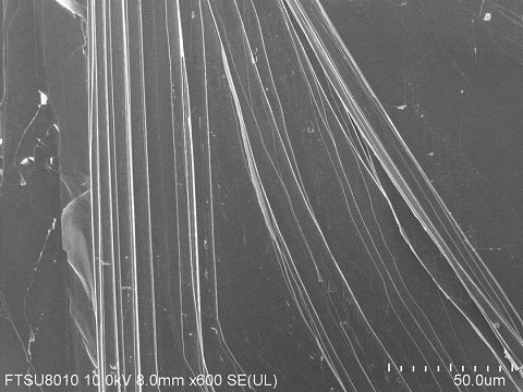
Layered van der Waals Structure: Enables easy exfoliation into thin layers for 2D materials research.
Topological Insulator Behavior: Exhibits protected surface states due to strong spin-orbit coupling, making it ideal for quantum applications.
High Carrier Mobility: Suitable for field-effect transistors (FETs) and nanoelectronic applications.
Thermoelectric Performance: Exhibits a high Seebeck coefficient and low thermal conductivity, making it useful for energy conversion applications.
Strong Optical Absorption: Efficient light absorption in the infrared and visible spectrum, suitable for optoelectronic devices.
Crystal Structure:
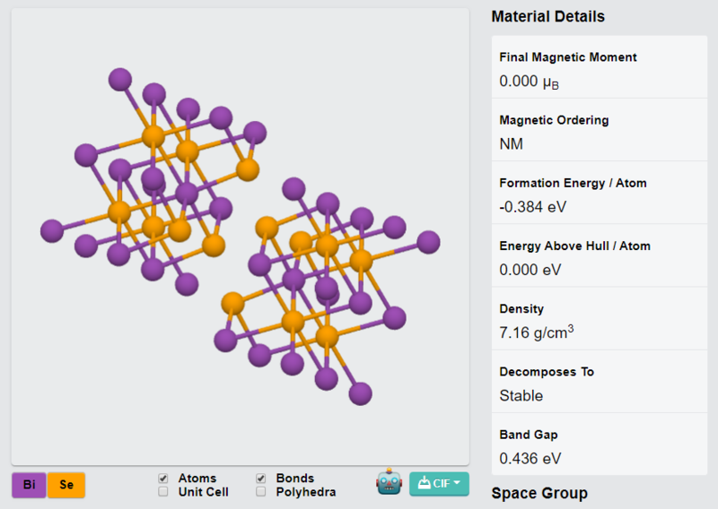
Type: Rhombohedral layered structure (R-3m space group)
Features: High crystallinity with uniform, defect-free layers, ideal for thin-film fabrication and nanoscale device integration.
Degree of Exfoliation:
Ease of Use: Easily exfoliated into monolayers or few-layer nanosheets for advanced material research and heterostructure integration.
Other Characteristics:
Efficient Charge Transport: High electrical conductivity for electronic and thermoelectric devices.
Environmental Stability: Maintains structural integrity under ambient conditions. Quantum
Applications: Supports spin-polarized surface states, making it an essential material for spintronics and topological quantum computing.
Applications:
Spintronics & Quantum Computing:
Enables research on quantum Hall effects, spin transport, and next-generation computing technologies. Nanoelectronics:
High-performance material for transistors, memory devices, and flexible electronic circuits. Thermoelectric Power Generation & Cooling:
Ideal for Peltier coolers, thermoelectric generators, and energy-harvesting applications. Optoelectronics & Infrared Detection:
Suitable for photodetectors, IR sensors, and infrared light-emitting devices.
2D Material Studies:
Excellent for exfoliation into monolayers and integration into van der Waals heterostructures. Synthesis Method:
Chemical Vapor Transport (CVT): Ensures high-quality crystals with excellent purity, uniform thickness, and high structural integrity.
| Option 1 | > 10 mm², > 100 mm², > 25 mm² |
|---|
Related products
-
NiI₃ Crystals
Price range: £499.99 through £899.99 -
WSSe Crystals
Price range: £599.99 through £899.99 -
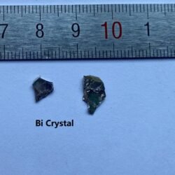
Bi Crystals
£499.99 -
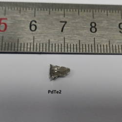
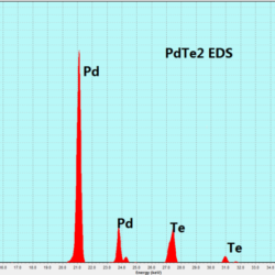
PdTe₂ Crystals
£499.99 -
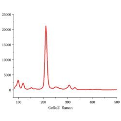
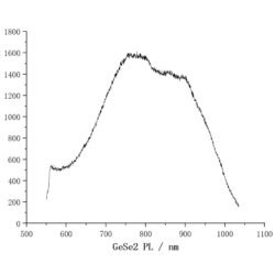
GeSe₂ Crystals
Price range: £499.99 through £569.99 -
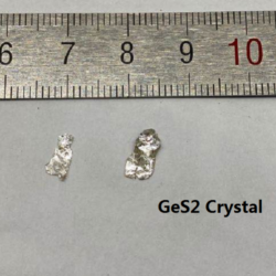
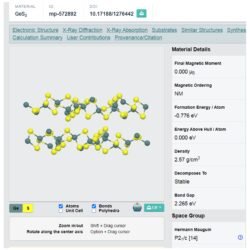
GeS₂ Crystals
Price range: £499.99 through £599.99 -
Ni₂Bi₂Te₅ Crystals
Price range: £499.99 through £569.99 -
ZrTe₃ Crystals
Price range: £499.99 through £599.99 -
GaS Crystals
Price range: £499.99 through £569.99 -

MoTe₂ Crystals (2H phase)
Price range: £499.99 through £569.99