
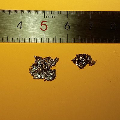
Nb-Doped MoSe₂ Crystals
Nb-doped MoSe₂ is a layered transition metal dichalcogenide (TMDC) with a van der Waals structure. Niobium doping introduces p-type conductivity, modifies the electronic band structure, and enhances the material’s optoelectronic and catalytic properties. These features make Nb-doped MoSe₂ an excellent candidate for spintronics, energy storage, and optoelectronic devices.
Sample Size Options:
Crystals larger than 10 mm²
Crystals larger than 25 mm²
Crystals larger than 100 mm²
Material Properties:
Layered van der Waals Structure: Facilitates exfoliation into thin layers for advanced research. P-Type Conductivity: Niobium doping introduces holes, enhancing charge transport dynamics.
Enhanced Catalytic Activity: High efficiency in hydrogen evolution reactions (HER) and electrocatalytic processes.
Tunable Bandgap: Niobium doping allows for bandgap modification to suit specific optoelectronic applications.
Crystal Structure:
Type: Hexagonal layered structure
Features: Cleavable layers suitable for thin-film fabrication and nanoscale studies.
Degree of Exfoliation:
Ease of Use: Readily exfoliates into monolayers or few-layer sheets for advanced material research.
Other Characteristics:
Quantum Potential: Enables studies on doping-induced quantum transport and electronic phenomena.
Optoelectronic Properties: Strong photoluminescence and high carrier mobility for advanced devices. Energy
Applications: Promising for catalytic and energy conversion technologies.
Applications:
Optoelectronics:
Ideal for photodetectors, light-emitting diodes, and photovoltaic devices. Quantum Materials Research:
Enables studies of quantum phenomena and p-type doping effects in TMDCs. Energy
Applications:
High catalytic performance for HER and other energy conversion processes.
2D Material Studies:
Perfect for integration into van der Waals heterostructures and thin-film devices. Spintronics:
Suitable for exploring spin-based devices and interactions in doped TMDCs.
| Option 1 | > 10 mm², > 100 mm², > 25 mm² |
|---|
Related products
-
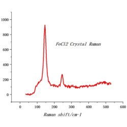
FeCl₂ Crystals
Price range: £499.99 through £569.99 -
NiI₃ Crystals
Price range: £499.99 through £899.99 -
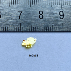
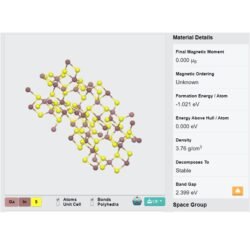
InGaS₃ Crystals
£499.99 -
BiI₃ Crystals
Price range: £499.99 through £899.99 -
FeBr₃ Crystals
Price range: £469.99 through £499.99 -
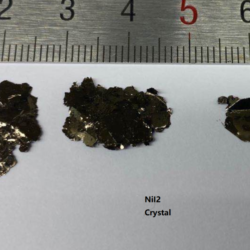
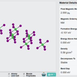
NiI₂ Crystals
Price range: £499.99 through £998.99 -
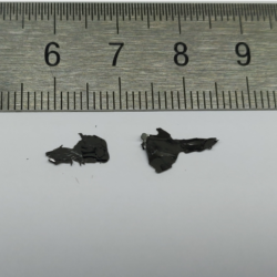
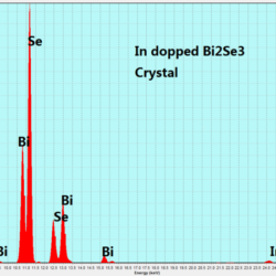
InBiSe₃ Crystals
Price range: £499.99 through £899.99 -
WSeTe Crystals
Price range: £599.99 through £899.99 -
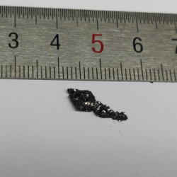
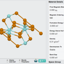
ZrTe₃ Crystals
Price range: £499.99 through £599.99 -
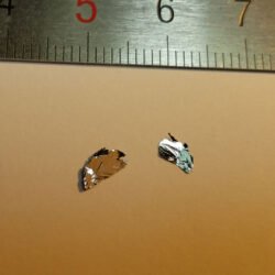
MoTe₂ Crystals (2H phase)
Price range: £499.99 through £569.99