Showing 97–112 of 249 results
-
$668.25
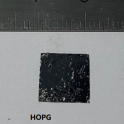
HOPG is a high-purity form of graphite with highly oriented layers, making it an the material for graphene exfoliation and specialized research applications. Its high crystallinity and layer uniformity permits consistent production of quality graphene sheets. Our HOPG samples are specially prepared to has high surface quality, with consistent results for graphene exfoliation and related…
-
$696.09 – $793.55Price range: $696.09 through $793.55
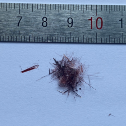
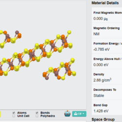
In₂GaBi₂S₆ Crystals In₂GaBi₂S₆ is a layered chalcogenide material with a van der Waals structure, combining unique semiconducting and optoelectronic properties. Its strong light absorption, variable bandgap, and high behavior make it a promising material for applications in optoelectronics, energy conversion, and specialized 2D material studies. Our In₂GaBi₂S₆ crystals are synthesized using the Chemical Vapor Transport…
-
$696.09 – $1,531.42Price range: $696.09 through $1,531.42
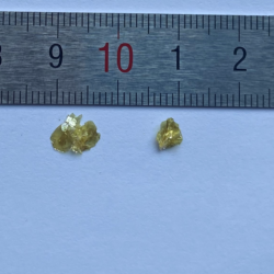
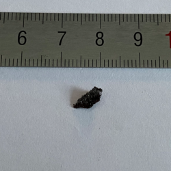
In₂P₃S₉ Crystals In₂P₃S₉ is a layered thiophosphate material with a van der Waals structure, exhibiting unique semiconducting and optical properties. Its high optical absorption, variable bandgap, and high behavior make it a promising material for optoelectronics, energy storage, and specialized 2D material research. Our In₂P₃S₉ crystals are synthesized using the Chemical Vapor Transport (CVT) method…
-
$696.09 – $793.55Price range: $696.09 through $793.55
In₂P₃Se₉ Crystals In₂P₃Se₉ is a layered ternary chalcogenide material with a van der Waals structure. It exhibits semiconducting behavior, strong optical absorption, and high environmental behavior, making it an high candidate for optoelectronics, energy storage, and 2D material studies. Sample Size Options: Crystals larger than 10 mm² Crystals larger than 25 mm² Material Properties: Layered…
-
$696.09 – $1,252.98Price range: $696.09 through $1,252.98
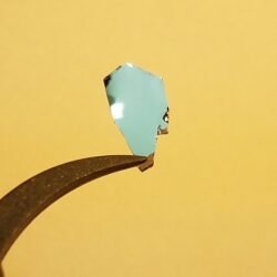
In₂Se₃ Crystals (α-2H Phase) In₂Se₃ is a layered semiconductor with a van der Waals structure, described for its variable electronic properties, phase-dependent behavior, and ferroelectric characteristics. The α-2H phase of In₂Se₃ exhibits high optical and electrical properties, making it applicable for applications in optoelectronics, memory devices, and 2D material studies. Our In₂Se₃ crystals are synthesized…
-
$696.09 – $793.55Price range: $696.09 through $793.55
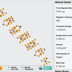
In₂Te₅ Crystals In₂Te₅ is a layered semiconductor material with a van der Waals structure, has its unique electronic, optical, and thermoelectric properties. Its anisotropic characteristics and narrow bandgap make it an high candidate for applications in optoelectronics, energy storage, and quantum materials research. Our In₂Te₅ crystals are synthesized using the Chemical Vapor Transport (CVT) method,…
-
$696.09 – $793.55Price range: $696.09 through $793.55
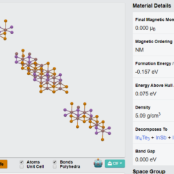
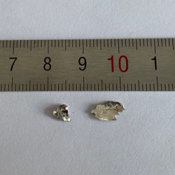
In₃SbTe₂ Crystals In₃SbTe₂ is a layered ternary chalcogenide material with unique electronic, optical, and thermoelectric properties. Its strong thermoelectric performance, variable electronic behavior, and layered structure make it an high candidate for specialized materials research, energy applications, and 2D material studies. Our In₃SbTe₂ crystals are synthesized using the Chemical Vapor Transport (CVT) method to with…
-
$696.09 – $793.55Price range: $696.09 through $793.55
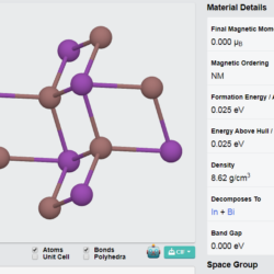
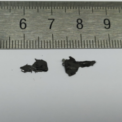
InBi Crystals InBi is a binary intermetallic compound with unique electronic, thermal, and optical properties. Its high electrical conductivity, low thermal conductivity, and semimetallic behavior make it an high material for quantum materials research, optoelectronics, and thermoelectric applications. Our InBi crystals are synthesized using the Chemical Vapor Transport (CVT) method, with high purity, precise stoichiometry,…
-
$696.09 – $1,252.98Price range: $696.09 through $1,252.98
InBiSe₃ Crystals InBiSe₃ is a layered ternary chalcogenide material with a van der Waals structure, exhibiting unique electronic, optical, and thermal properties. With a variable bandgap and strong anisotropic behavior, InBiSe₃ is a promising candidate for applications in optoelectronics, energy storage, and specialized 2D material research. Sample Size Options: Crystals larger than 10 mm² Crystals…
-
$696.09
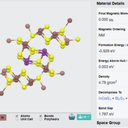
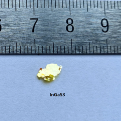
InGaS₃ Crystals InGaS₃ is a ternary layered chalcogenide material with a van der Waals structure, semiconducting properties, and optical absorption. Its electronic and optical behavior can be tuned for optoelectronics, energy applications, and 2D material studies. Sample Size Options: Crystals larger than 10 mm² Material Properties: Layered Structure: Facilitates exfoliation into thin layers for 2D…
-
$835.32 – $952.26Price range: $835.32 through $952.26
InSb Crystals InSb is a narrow bandgap semiconductor with strong electronic, optical, and thermoelectric properties. Its high electron mobility, strong infrared sensitivity, and low thermal conductivity make it a premier material for infrared detectors, high-speed electronics, and quantum materials research. Our InSb crystals are synthesized using the Chemical Vapor Transport (CVT) method to with high…
-
$696.09 – $1,252.98Price range: $696.09 through $1,252.98
InSe Crystals InSe (γ-phase Indium Selenide) is a layered van der Waals semiconductor that exhibits optoelectronic, electronic, and thermoelectric properties. It features a variable bandgap, high carrier mobility, and strong light absorption, making it applicable to applications in photodetectors, field-effect transistors (FETs), photovoltaics, and nonlinear optics. Our InSe (γ-phase) crystals are synthesized using the Chemical…
-
$696.09 – $793.55Price range: $696.09 through $793.55
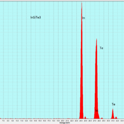
InSiTe₃ Crystals InSiTe₃ is a layered chalcogenide material with a van der Waals structure, has its unique electronic, optical, and thermoelectric properties. Its variable bandgap, high thermoelectric performance, and high behavior make it a promising material for optoelectronics, energy storage, and specialized 2D material research. Our InSiTe₃ crystals are synthesized using the Chemical Vapor Transport…
-
$835.32
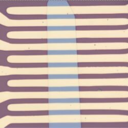
Mechanically Exfoliated Black Phosphorus FET Device Black Phosphorus (BP) FET Device Device Structure: Highly Doped Conductive Si Substrate / 300 nm SiO₂ Layer / Au Electrodes / Mechanically Exfoliated Few-Layer Black Phosphorus Device Specifications: Channel Width: 5 µm Few-Layer Black Phosphorus (BP) For specific thickness requirements, please contact us. Device Description & Features: High-Mobility 2D…
-
$835.32
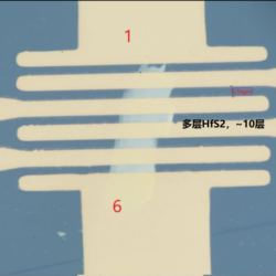
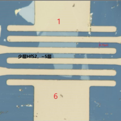
Mechanically Exfoliated HfS₂ FET Device Device Structure: Au Electrodes / HfS₂ / 300 nm SiO₂ / Si Back-Gated FET HfS₂ Layer Options: Few-layer (~5 layers) Multilayer (~10 layers) For specific thickness requirements, please contact us. Device Description & Features: High-Mobility 2D Semiconductor: Hafnium disulfide (HfS₂) is a layered transition metal dichalcogenide (TMD) with high electron…
-
$835.32
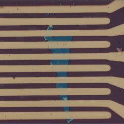
Mechanically Exfoliated Monolayer Graphene FET Device Structure: Highly Doped Conductive Si Substrate / 300 nm SiO₂ Layer / Monolayer Graphene / Cr+Au Electrodes Device Specifications: Graphene Thickness: Monolayer Electrode Material: Cr+Au Gate Dielectric: 300 nm SiO₂ Applications include specific device modifications, please contact us. Device Description & Features: Ultra-High Carrier Mobility: Graphene exhibits ballistic transport,…