
InSe Crystals
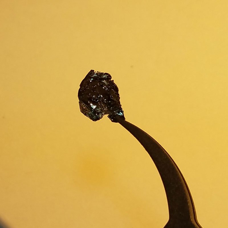
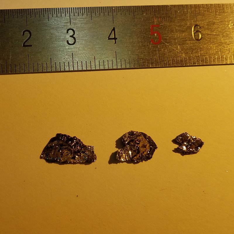
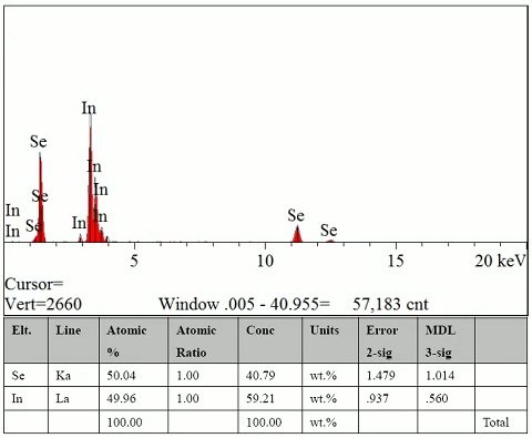
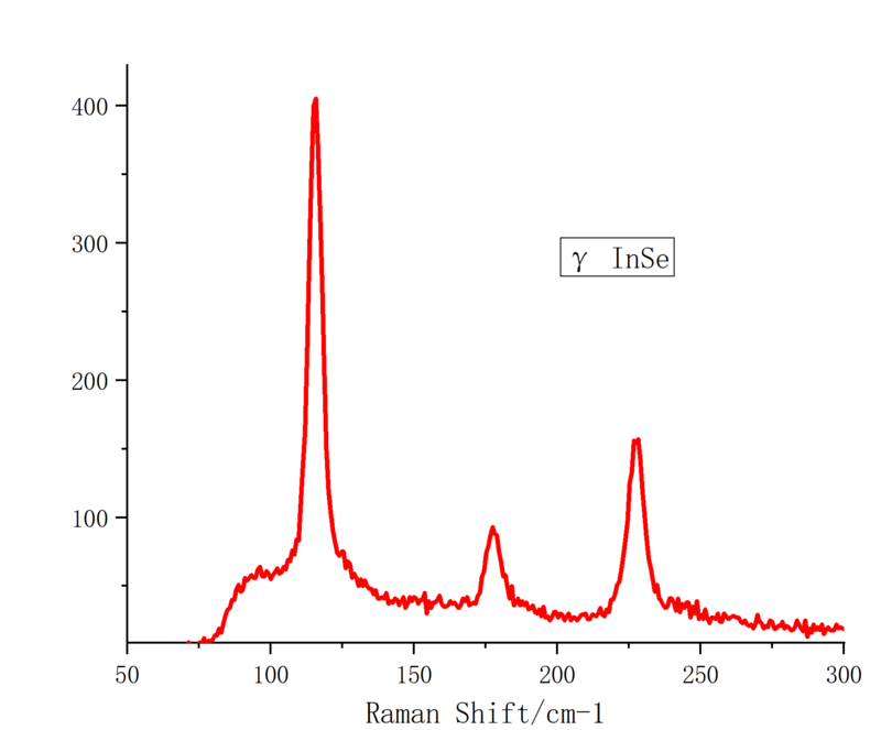
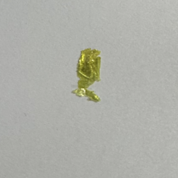
InSe (γ-phase Indium Selenide) is a layered van der Waals semiconductor that exhibits optoelectronic, electronic, and thermoelectric properties. It features a variable bandgap, high carrier mobility, and strong light absorption, making it applicable to applications in photodetectors, field-effect transistors (FETs), photovoltaics, and nonlinear optics. Our InSe (γ-phase) crystals are synthesized using the Chemical Vapor Transport (CVT) method, with high purity, strong crystallinity, and well-controlled stoichiometry.
Sample Size Options:
Crystals larger than 10 mm²
Crystals larger than 25 mm²
Crystals larger than 100 mm²
Material Properties:
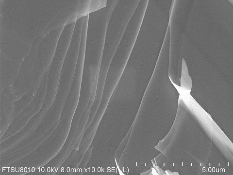
Layered van der Waals Structure: Permits facile exfoliation into monolayers or few-layer nanosheets for 2D material studies.
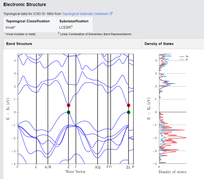
Variable Bandgap: Exhibits a direct bandgap of ~1.2 eV in bulk, shifting to ~1.8 eV in monolayer form, applicable to optoelectronic applications.
High Carrier Mobility: Demonstrates strong electron mobility compared to conventional TMDs, making it applicable for high-speed electronic devices.
Strong Optical Absorption: High-efficiency absorption in the visible and near-infrared spectrum, enhancing its potential for photodetectors and solar cells.
Nonlinear Optical Properties: Displays strong second-harmonic generation (SHG) effects, making it a promising material for frequency conversion.
Crystal Structure:
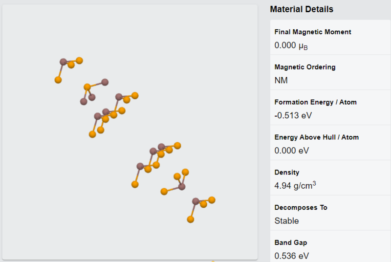
Type: γ-phase (hexagonal layered structure)
Features: High crystallinity with uniform, defect-free layers, applicable to thin-film fabrication and device applications.
Degree of Exfoliation:
Ease of Use: Can be easily exfoliated into monolayers or few-layer nanosheets for specialized materials research and van der Waals heterostructure assembly.
Other Characteristics:
Anisotropic Electrical Transport: Exhibits direction-dependent charge transport, applicable to specialized electronic and thermoelectric devices.
High behavior: Maintains its structural integrity under controlled conditions, permits long-term applications. Potential for Quantum Technologies: Applicable to quantum optics and valleytronic applications due to its electronic and optical characteristics.
Applications:
Optoelectronics:
Applicable for photodetectors, light-emitting diodes (LEDs), and photovoltaic devices due to strong light absorption and photoluminescence. Nanoelectronics:
Standard material for transistors, memory devices, and flexible electronics.
Nonlinear Optics: Applicable to frequency conversion and laser applications due to its second-harmonic generation (SHG) capabilities.
2D Material Studies:
Applicable for exfoliation into monolayers and assembly into van der Waals heterostructures. Sensors:
High sensitivity for gas detection, chemical sensing, and biosensing applications. Synthesis Method:
Chemical Vapor Transport (CVT): With quality crystals with purity, uniform thickness, and high structural integrity.
| Option 1 | > 10 mm², > 100 mm², > 25 mm² |
|---|
Related products
-
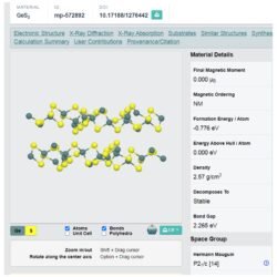
GeS₂ Crystals
Price range: $696.09 through $835.32 -
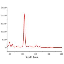
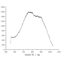
GeSe₂ Crystals
Price range: $696.09 through $793.55 -
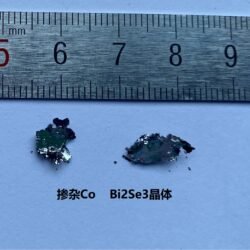
Co-Doped Bi₂Se₃ Crystals
$696.09 -
NiI₃ Crystals
Price range: $696.09 through $1,252.98 -
VS₂ Crystals
Price range: $696.09 through $793.55 -
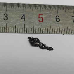
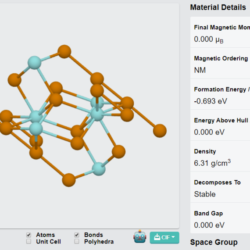
ZrTe₃ Crystals
Price range: $696.09 through $835.32 -
Ni₂Bi₂Te₅ Crystals
Price range: $696.09 through $793.55 -
RuCl₃ Crystals
Price range: $696.09 through $1,252.98 -
Te Crystals
$696.09 -
GaS Crystals
Price range: $696.09 through $793.55