-
$666.86
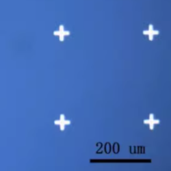
SiO₂ Alignment Cross Mark Wafer (Au Pattern on Si (100)) These alignment-mark silicon wafers feature photolithographically patterned gold cross markers fabricated on thermal silicon dioxide. The cross patterns provide spatial references for microscopy, microfabrication alignment, and microelectrode positioning. The patterned surface supports distance measurement and positioning in micro-scale experiments, and it is used for lithography…
-
$666.86 – $833.92Price range: $666.86 through $833.92
SiO₂ Alignment Mark Wafer (Cr Number Pattern on Si (100)) These thermal silicon dioxide wafers feature photolithographic chromium number patterns designed for alignment, localization, and microfabrication applications. The patterned surface provides indexed micro-scale positioning for electrochemical mapping, MEMS device development, lithography training, and microelectrode alignment. Wafer Specifications Diameter: 4 inch Orientation: Si (100) Resistivity: <…
-
$82.13 – $366.14Price range: $82.13 through $366.14
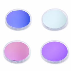
Thermal SiO₂ on N-Type (Arsenic-Doped) Si (100) Wafers Overview Our thermal silicon dioxide (SiO₂) wafers are fabricated using high-temperature thermal oxidation on heavily doped N-type (arsenic-doped) Si (100) substrates with ultra-low resistivity of 0.001–0.005 Ω·cm. The highly doped silicon substrate has high electrical conductivity, while the thermally grown SiO₂ layer has consistent film density, high…
-
$82.13 – $366.14Price range: $82.13 through $366.14
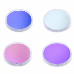
Thermal SiO₂ on N-Type (Phosphorus-Doped) Si (100) Wafers Overview Our thermal silicon dioxide (SiO₂) wafers are fabricated using high-temperature thermal oxidation on N-type (phosphorus-doped) Si (100) substrates with a resistivity range of 1–10 Ω·cm. Thermally grown oxide has consistent film density, high thickness uniformity, low interface trap density, and high dielectric strength compared to deposited…
-
$82.13 – $366.14Price range: $82.13 through $366.14
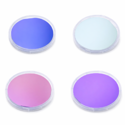
Thermal SiO₂ on P-Type (Boron-Doped) Si (100) Wafers Overview Our thermal silicon dioxide (SiO₂) wafers are fabricated using high-temperature thermal oxidation on P-type (boron-doped) Si (100) substrates. Available resistivity ranges include 1–10 Ω·cm and heavily doped 0.001–0.005 Ω·cm options. Thermally grown SiO₂ has consistent film density, high dielectric strength, and a consistent Si/SiO₂ interface compared…
-
$82.13 – $349.43Price range: $82.13 through $349.43
Thermal SiO₂ on Undoped Si (100) Wafers Overview Our thermal silicon dioxide (SiO₂) wafers are fabricated using high-temperature dry/wet thermal oxidation on undoped Si (100) substrates. Thermal oxide has consistent film density, high uniformity, low defect density, and consistent electrical insulation compared to deposited oxide films. These wafers are used in semiconductor research, MOS structure…