
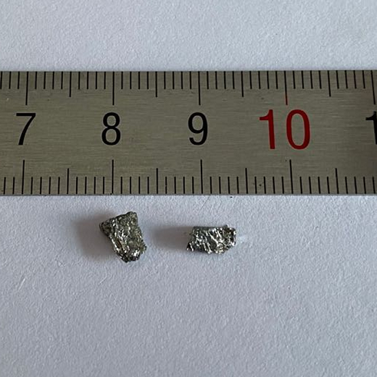
InSb Crystals
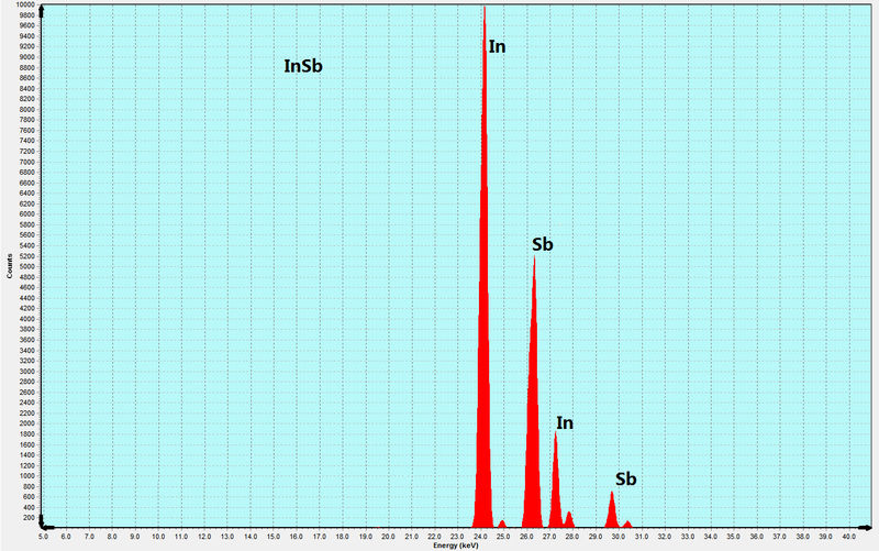
InSb is a narrow bandgap semiconductor with strong electronic, optical, and thermoelectric properties. Its high electron mobility, strong infrared sensitivity, and low thermal conductivity make it a premier material for infrared detectors, high-speed electronics, and quantum materials research. Our InSb crystals are synthesized using the Chemical Vapor Transport (CVT) method to with high purity, precise stoichiometry, and strong crystallinity for specialized applications.
Sample Size Options:
Crystals larger than 10 mm²
Crystals larger than 25 mm²
Material Properties:
Narrow Bandgap: Applicable to infrared detection and low-power electronics.
High Electron Mobility: High carrier mobility above 70,000 cm²/V-s.
Optical Absorption: Strong absorption in the infrared range, applicable for photonic applications.
Thermoelectric Potential: Low thermal conductivity for energy conversion applications.
Crystal Structure:
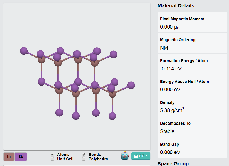
Type: Zinc-blende cubic structure
Features: Highly uniform and cleavable, applicable to thin-film fabrication and nanoscale research.
Degree of Exfoliation:
Ease of Use: Can be processed into thin films for specialized device applications.
Other Characteristics:
Infrared Sensitivity: Standard in infrared photodetectors and imaging systems. High-Speed Electronics: Applicable for applications requiring high carrier mobility and low power consumption.
Quantum Potential: Promising for quantum well structures and spintronic devices.
Applications:
Infrared Optoelectronics:
Applicable for photodetectors, thermal imaging, and spectroscopy applications. High-Speed Electronics:
Applicable to transistors, Hall sensors, and other electronic devices requiring high mobility. Quantum Materials Research:
Permits exploration of quantum transport, spin-orbit coupling, and topological phenomena. Energy
Applications:
Promising for thermoelectric energy harvesting and cooling systems. Sensors:
High sensitivity to environmental and magnetic fields, applicable to specialized sensing technologies.
| Option 1 | > 10 mm², > 25 mm² |
|---|
Related products
-
VS₂ Crystals
Price range: $696.09 through $793.55 -
NiI₃ Crystals
Price range: $696.09 through $1,252.98 -
TiS₃ Crystals
Price range: $654.33 through $1,252.98 -
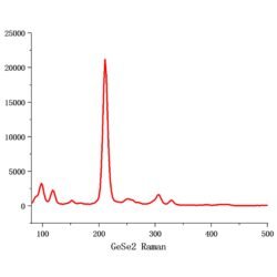
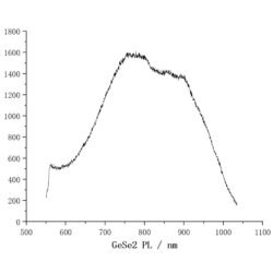
GeSe₂ Crystals
Price range: $696.09 through $793.55 -
FeBr₃ Crystals
Price range: $654.33 through $696.09 -
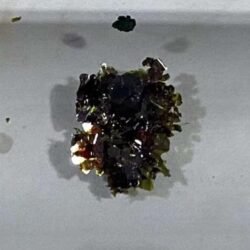
CrBr₃ Crystals
$696.09 -
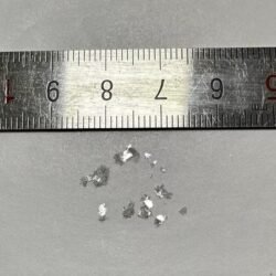
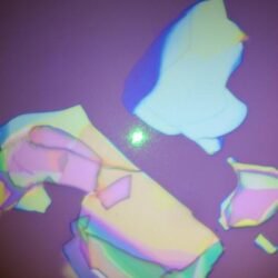
BiOCl Crystals
Price range: $696.09 through $793.55 -
RuCl₃ Crystals
Price range: $696.09 through $1,252.98 -
Co-Doped Bi₂Se₃ Crystals
$696.09 -
GaS Crystals
Price range: $696.09 through $793.55