Showing 641–656 of 1232 results
-
£610.99 – £766.99Price range: £610.99 through £766.99
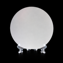
Magnesium Oxide (MgO) Single Crystal Wafer Physical Properties: – Crystal Structure: Cubic System – Lattice Constant: a = 4.216 Angstrom – Density: 3.58 g/cm³ – Melting Point: 2852 °C – Mohs Hardness: 5.5 – Growth Method: Arc Fusion Standard Specifications: – Orientation Accuracy: (100) < 0.3°; (110)/(111) < 0.5° – Surface Roughness: Ra < 0.5…
-
£350.99 – £753.99Price range: £350.99 through £753.99
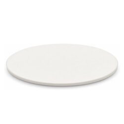
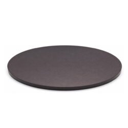
Magnesium Oxide (MgO) Sputtering Target, 99.99% Purity, Circular Nanostore’s Magnesium Oxide (MgO) sputtering target is a 99.99% purity oxide ceramic PVD source material for magnetron sputtering, ion sputtering, and laboratory thin-film deposition. It is supplied in circular target formats for research, development, and small-batch process work where clean handling, dimensional consistency, and reliable material identity…
-
£128.99 – £149.99Price range: £128.99 through £149.99
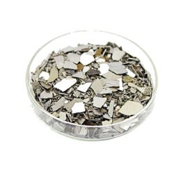
Manganese (Mn) Pellets, 99.8% Purity Nanostore Manganese (Mn) pellets are high-purity source materials supplied for thin-film deposition research, evaporation source loading, alloy preparation, and laboratory materials development. The pellet and piece formats are convenient for weighing, loading, and small-batch experimental workflows where material identity, purity selection, and clean handling are important. Key Features High-Purity Elemental…
-
£278.99 – £1,113.99Price range: £278.99 through £1,113.99
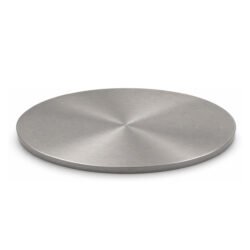
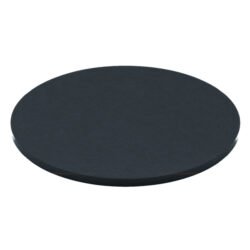
Manganese (Mn) Sputtering Target, 99.9% Purity, Circular Nanostore’s Manganese (Mn) sputtering target is a 99.9% purity high-purity transition metal PVD source material for magnetron sputtering, ion sputtering, and laboratory thin-film deposition. It is supplied in circular target formats for research, development, and small-batch process work where clean handling, dimensional consistency, and reliable material identity are…
-
£154.99 – £322.99Price range: £154.99 through £322.99
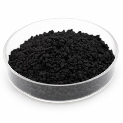
Manganese Dioxide (MnO₂) Evaporation Pellets, 99.99% Purity Nanostore Manganese Dioxide (MnO₂) evaporation pellets are high-purity compound source materials supplied for evaporation coating, thin-film deposition research, optical and functional films, and laboratory PVD process development. The pellet format is convenient for weighing, source loading, and small-batch experimental workflows where clean handling and controlled material identity are…
-
£395.99 – £959.99Price range: £395.99 through £959.99
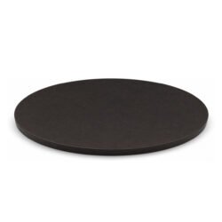
Manganese Dioxide (MnO₂) Sputtering Target, 99.99% Purity, Circular Nanostore’s Manganese Dioxide (MnO₂) sputtering target is a 99.99% purity transition-metal oxide ceramic PVD source material for magnetron sputtering, ion sputtering, and laboratory thin-film deposition. It is supplied in circular target formats for research, development, and small-batch process work where clean handling, dimensional consistency, and reliable material…
-
Price upon request
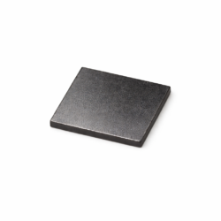
Manganese Monoxide (MnO) Single Crystal Substrate Physical Properties: – Crystal Structure: Cubic System – Lattice Constant: a = 4.43 Angstrom – Melting Point: 1945 °C – Density: 5.43 g/cm³ – Color: dark green
-
£1,306.99
Manganese Selenide (MnSe) Sputtering Target, 99.9% Purity, Mn:Se 1:1 at%, Circular Nanostore’s Manganese Selenide (MnSe) sputtering target is a 99.9% purity, mn:se 1:1 at% compound chalcogenide PVD source material for magnetron sputtering, ion sputtering, and laboratory thin-film deposition. It is supplied in circular target formats for research, development, and small-batch process work where clean handling,…
-
Price upon request
Manganese Telluride Alloy (MnTe) Sputtering Target, 99.9% Purity, Mn:Te = 1:1.3 at%, Circular (Price Upon Request) Nanostore’s Manganese Telluride Alloy (MnTe) sputtering target is a 99.9% purity, mn:te = 1:1.3 at% custom chalcogenide alloy PVD source material for magnetron sputtering, ion sputtering, and laboratory thin-film deposition. It is supplied in circular target formats for research,…
-
£46.99
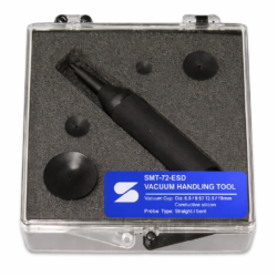
Manual Vacuum Suction Pen (SMT72-ESD) Application: Designed for precision handling in laboratories and SMT assembly. Ideal for picking up electronic components, lenses, and chips without direct contact, preventing contamination and damage. Key Features: * Advanced Technology: Utilizes technology referencing US MTI standards with a unique suction cup structure for reliable handling. * ESD Safe Material…
-
£599.99
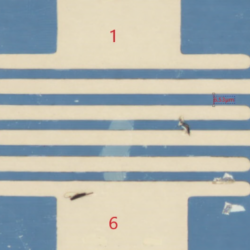
Mechanically Exfoliated Black Phosphorus FET Device Black Phosphorus (BP) FET Device Device Structure: Highly Doped Conductive Si Substrate / 300 nm SiO₂ Layer / Au Electrodes / Mechanically Exfoliated Few-Layer Black Phosphorus Device Specifications: Channel Width: 5 µm Few-Layer Black Phosphorus (BP) For specific thickness requirements, please contact us. Device Description & Features: High-Mobility 2D…
-
£599.99
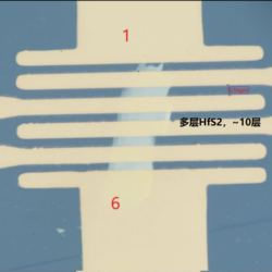
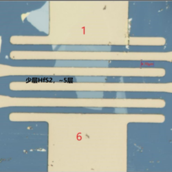
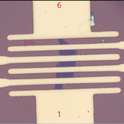
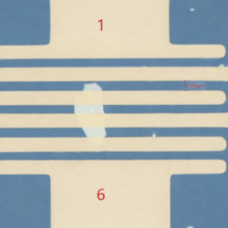
Mechanically Exfoliated HfS₂ FET Device Device Structure: Au Electrodes / HfS₂ / 300 nm SiO₂ / Si Back-Gated FET HfS₂ Layer Options: Few-layer (~5 layers) Multilayer (~10 layers) For specific thickness requirements, please contact us. Device Description & Features: High-Mobility 2D Semiconductor: Hafnium disulfide (HfS₂) is a layered transition metal dichalcogenide (TMD) with high electron…
-
£599.99
Mechanically Exfoliated Monolayer Graphene FET Device Structure: Highly Doped Conductive Si Substrate / 300 nm SiO₂ Layer / Monolayer Graphene / Cr+Au Electrodes Device Specifications: Graphene Thickness: Monolayer Electrode Material: Cr+Au Gate Dielectric: 300 nm SiO₂ For specific device modifications, please contact us. Device Description & Features: Ultra-High Carrier Mobility: Graphene exhibits ballistic transport, extremely…
-
£599.99
Mechanically Exfoliated ReS₂ FET Device ReS₂ FET (Back-Gated ReS₂ FET) Device Structure: Au Electrodes / ReS₂ / 300 nm SiO₂ / Si Back-Gated FET Device Specifications: Channel Width: 5 µm Few-layer (~5 layers) Multilayer (~10 layers) For specific thickness requirements, please contact us. Device Description & Features: Anisotropic 2D Semiconductor: Rhenium disulfide (ReS₂) is a…
-
£599.99
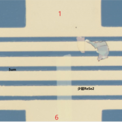
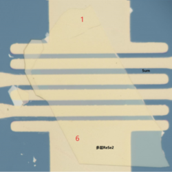
Mechanically Exfoliated ReSe₂ FET Device ReSe₂ FET (Back-Gated ReSe₂ FET) Device Structure: Au Electrodes / ReSe₂ / 300 nm SiO₂ / Si Back-Gated FET ReSe₂ Layer Options: Few-layer (~5 layers) Multilayer (~10 layers) For specific thickness requirements, please contact us. Device Description & Features: Anisotropic 2D Semiconductor: Rhenium diselenide (ReSe₂) is a layered transition metal…
-
£599.99
Mechanically Exfoliated WS₂ FET Device WS₂ FET (Back-Gated WS₂ FET) Device Structure: Au Electrodes / WS₂ / 300 nm SiO₂ / Si Back-Gated FET WS₂ Layer Options: Monolayer Few-layer ( ~5 layers) Multilayer (~10 layers) For specific thickness requirements, please contact us. Device Description & Features: High-Performance 2D Semiconductor: Tungsten disulfide (WS₂) is a layered…