
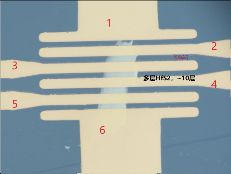
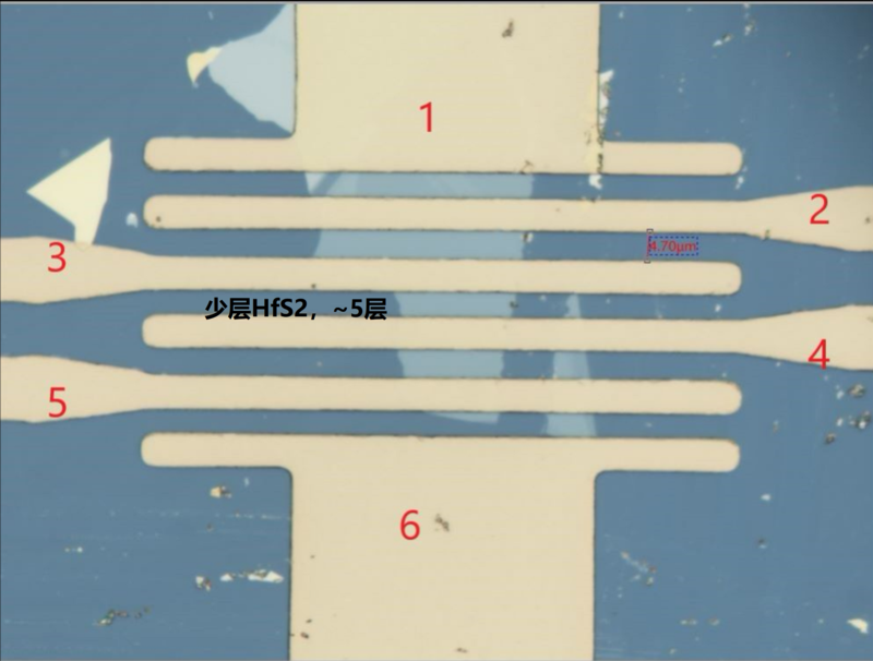
Mechanically Exfoliated HfS₂ FET Device
Device Structure:
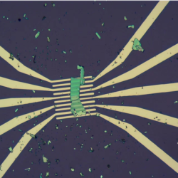
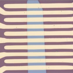
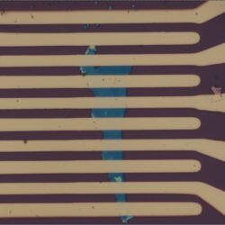
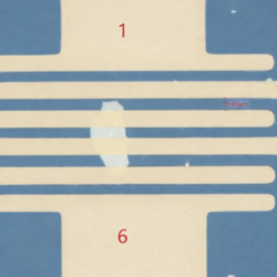
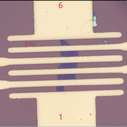
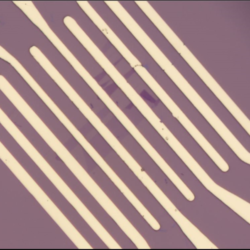
Au Electrodes / HfS₂ / 300 nm SiO₂ / Si Back-Gated FET
HfS₂ Layer Options:
Few-layer (~5 layers)
Multilayer (~10 layers)
For specific thickness requirements, please contact us.
Device Description & Features:
High-Mobility 2D Semiconductor: Hafnium disulfide (HfS₂) is a layered transition metal dichalcogenide (TMD) with high electron mobility, making it a promising material for next-generation field-effect transistors (FETs). Back-Gated Configuration: The SiO₂/Si back-gate structure enables efficient gate control over the channel conductivity, facilitating low-power and high-performance electronic applications.
Mechanically Exfoliated Layers: Ensures high-quality, defect-free HfS₂ films with well-preserved intrinsic electronic properties.
Gold Electrodes: Ohmic contacts for efficient charge injection, optimizing device performance.
Tunable Thickness: Different layer numbers allow for studying thickness-dependent electronic properties.
Applications:
High-Performance Field-Effect Transistors (FETs):
HfS₂-based FETs exhibit high carrier mobility and excellent gate tunability. Flexible and Low-Power Electronics:
Thin-film HfS₂ FETs are ideal for wearable and flexible electronic devices. Optoelectronic Devices:
HfS₂ exhibits a tunable bandgap and strong light absorption, making it suitable for photodetectors. Quantum & Neuromorphic Computing:
Potential use in low-dimensional quantum transport studies and next-generation neuromorphic computing architectures.
| Option 1 | Few-layer (~5 layers), Multilayer (~10 layers) |
|---|
Related products
-
-

Monolayer 2H-MoTe₂ FET Device
£599.99 -
Multilayer ReS₂/PdSe₂ FET Device
£599.99 -
-
-
-
WS₂ FET Device
£599.99 -
MoS₂ FET Device
£599.99 -
-
Graphene FET Device
£599.99