
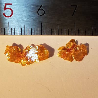
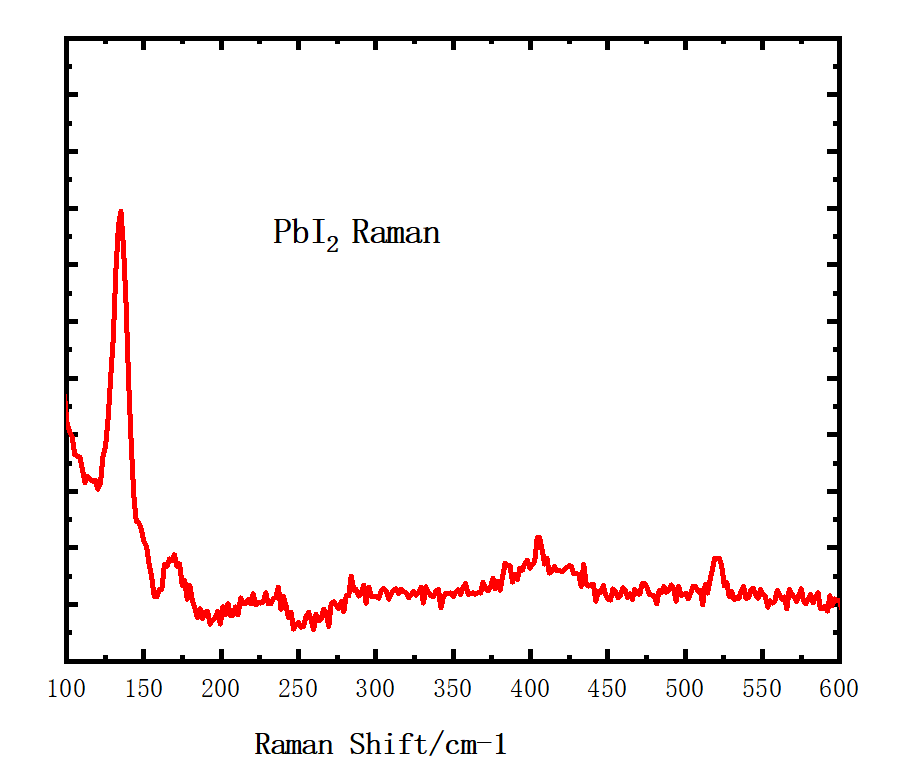
PbI₂ Crystals
PbI₂ is a layered halide material with a van der Waals structure, known for its wide bandgap, high photoconductivity, and excellent optical properties. It is widely used in optoelectronic devices, photodetectors, and as a precursor material for perovskite solar cells.
Sample Size Options:
Crystals larger than 10 mm²
Crystals larger than 25 mm²
Crystals larger than 100 mm²
Material Properties:
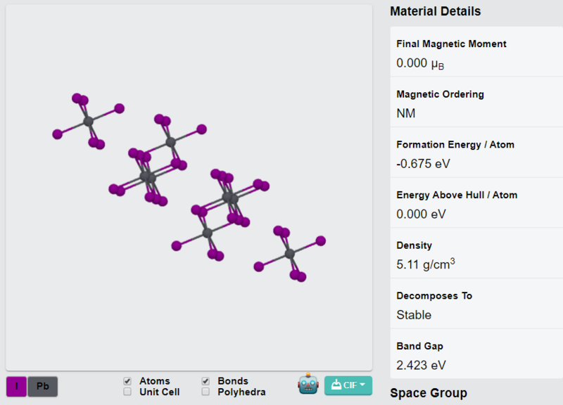
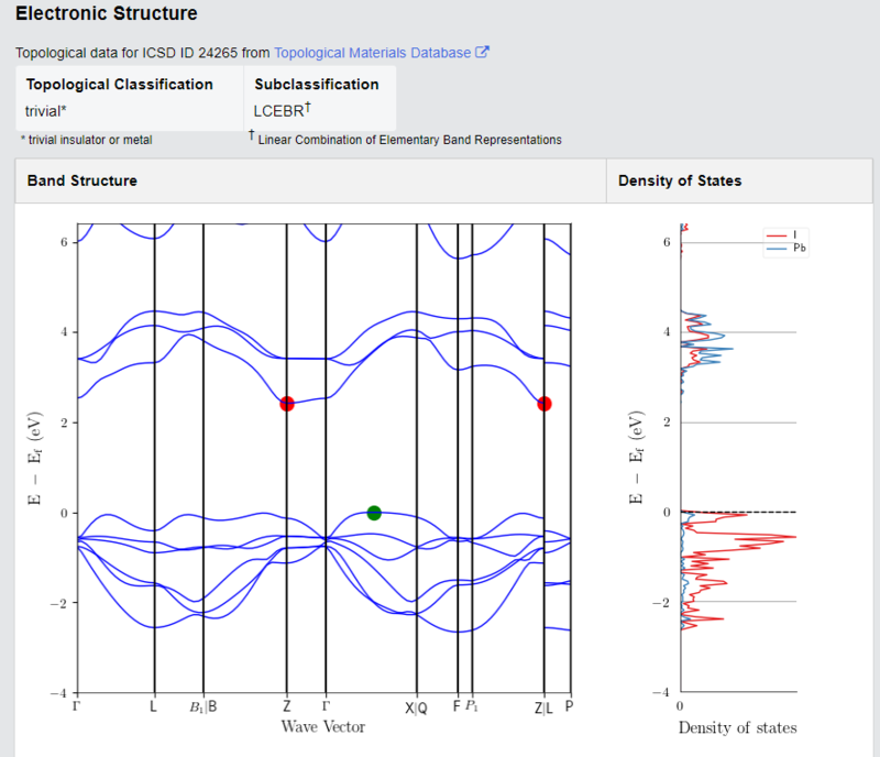
Layered van der Waals Structure: Facilitates exfoliation into monolayers or few-layer sheets for advanced material studies. Wide Bandgap (~2.3 eV): Suitable for optoelectronic and photonic applications.
High Photoconductivity: Ideal for light-sensitive devices and detectors. Thermal and Chemical Stability: Maintains performance under controlled conditions.
Crystal Structure:
Type: Hexagonal layered structure
Features: Cleavable layers suitable for thin-film fabrication and nanoscale research.
Degree of Exfoliation:
Ease of Use: Readily exfoliates into thin layers for advanced research and applications.
Other Characteristics:
Optoelectronic Potential: Excellent photoluminescence and optical absorption for cutting-edge applications.
Photodetector Performance: High light sensitivity in the UV-visible range. Energy
Applications: Serves as a precursor for perovskite solar cell fabrication.
Applications:
Optoelectronics:
Ideal for photodetectors, light-emitting devices, and photovoltaic cells. Photonic Devices:
High potential for waveguides, lasers, and UV light sensors. Energy
Applications:
Used as a precursor material for perovskite solar cells and energy conversion systems.
2D Material Studies:
Perfect for exfoliation into thin layers and integration into van der Waals heterostructures. Quantum Materials Research:
Enables exploration of quantum confinement and electronic properties in layered halides. Synthesis Method:
| Option 1 | > 10 mm², > 100 mm², > 25 mm² |
|---|
Related products
-
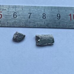
Ni₂Bi₂Te₅ Crystals
Price range: £499.99 through £569.99 -
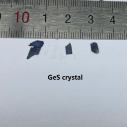
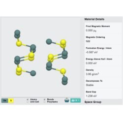
GeS Crystals
Price range: £499.99 through £549.99 -
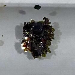
CrBr₃ Crystals
£499.99 -
FeBr₃ Crystals
Price range: £469.99 through £499.99 -
VS₂ Crystals
Price range: £499.99 through £569.99 -
FeCl₃ Crystals
Price range: £499.99 through £899.99 -
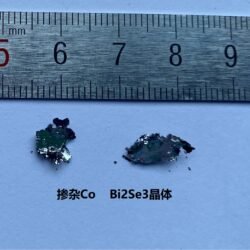
Co-Doped Bi₂Se₃ Crystals
£499.99 -
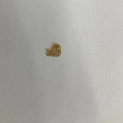
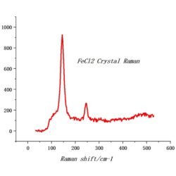
FeCl₂ Crystals
Price range: £499.99 through £569.99 -
BiI₃ Crystals
Price range: £499.99 through £899.99 -
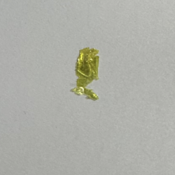
GaS Crystals
Price range: £499.99 through £569.99