
NbSe₂ Crystals
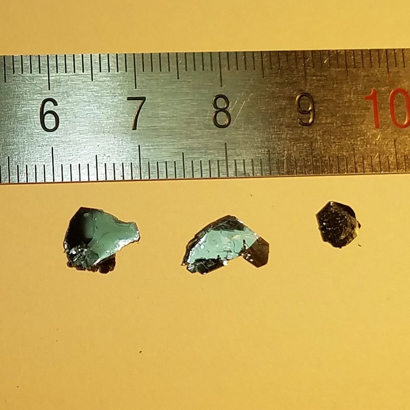
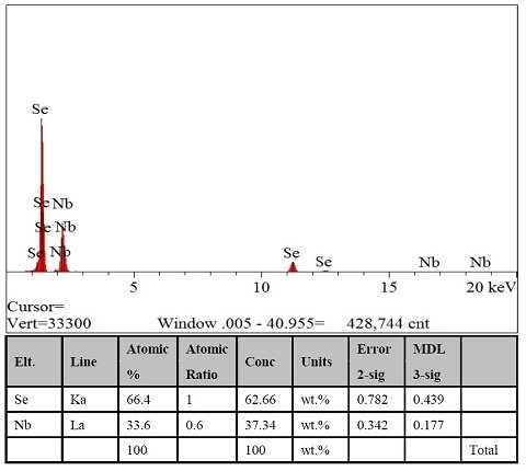
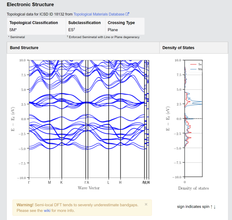
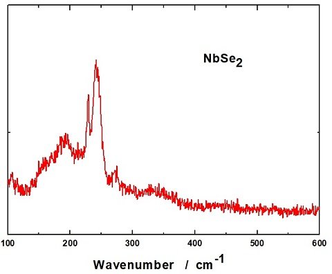
NbSe₂ (Niobium Diselenide) is a layered transition metal dichalcogenide (TMD) that exhibits both superconducting and charge density wave (CDW) behaviors. It is widely studied for its potential applications in nanoelectronics, spintronics, superconducting circuits, and quantum materials research. With strong spin-orbit coupling, tunable electronic properties, and excellent environmental stability, NbSe₂ is an ideal material for advanced technological applications. Our NbSe₂ crystals are synthesized using the Chemical Vapor Transport (CVT) method, ensuring high purity, superior crystallinity, and precise stoichiometry.
Sample Size Options:
Crystals larger than 10 mm²
Crystals larger than 25 mm²
Crystals larger than 100 mm²
Material Properties:
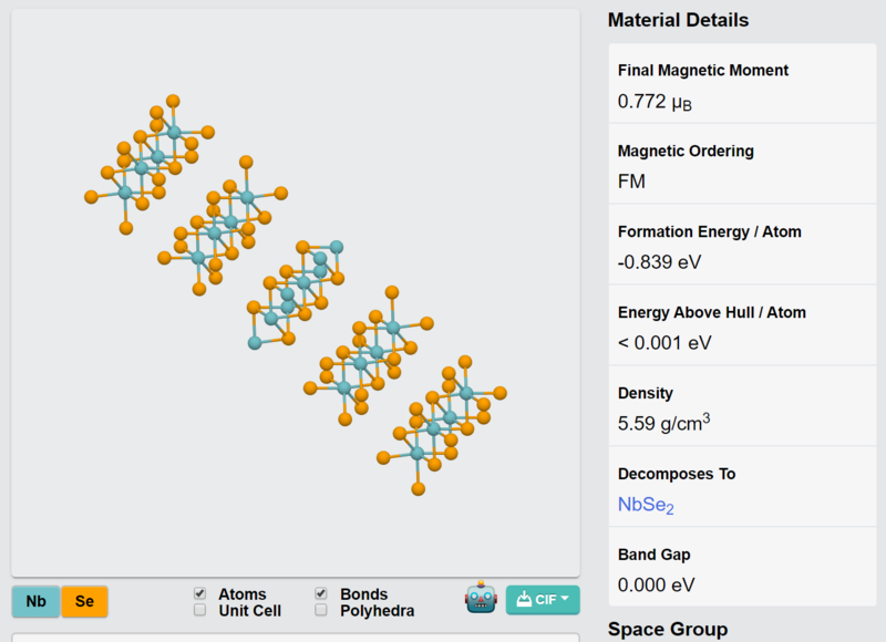
Layered van der Waals Structure: Enables facile exfoliation into monolayers or few-layer nanosheets for 2D material research.
Superconducting Properties: Exhibits superconductivity below ~7.2 K, making it ideal for quantum devices. Charge Density Wave (CDW) Behavior: Strong electron-lattice interactions lead to CDW phase transitions.
High Carrier Mobility: Suitable for nanoelectronic and quantum computing applications. Spin-Orbit Coupling: Enables valleytronic and spintronic applications.
Excellent Environmental Stability: Maintains structural integrity under ambient conditions.
Crystal Structure:
Type: Hexagonal (2H phase) layered structure
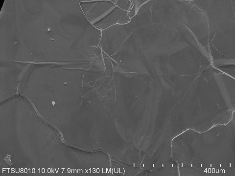
Features: High crystallinity with uniform, defect-free layers, ideal for thin-film fabrication and nanoscale device applications.
Degree of Exfoliation:
Ease of Use: Easily exfoliated into monolayers or few-layer nanosheets for advanced material research and heterostructure integration.
Other Characteristics:
Anisotropic Transport Properties: Exhibits direction-dependent charge transport, suitable for novel electronic and thermoelectric devices.
Quantum Confinement Effects: Exhibits strong light-matter interactions in monolayer form. Potential for Topological Superconductivity: Making it an exciting candidate for Majorana fermion research.
Applications:
Superconducting Quantum Circuits:
Ideal for low-temperature superconducting electronics and quantum computing. Nanoelectronics:
High-performance material for transistors, memory devices, and flexible electronic circuits. Spintronics & Quantum Materials Research:
Enables research on spin-orbit coupling, valley polarization, and charge density wave effects.
2D Material Studies:
Perfect for exfoliation into monolayers and integration into van der Waals heterostructures. Sensors & Catalysis:
High sensitivity for gas detection, chemical sensing, and electrocatalytic applications. Synthesis Method:
Chemical Vapor Transport (CVT): Ensures high-quality crystals with excellent purity, uniform thickness, and high structural integrity.
| Option 1 | > 10 mm², > 100 mm², > 25 mm² |
|---|
Related products
-
GeS Crystals
Price range: £499.99 through £549.99 -
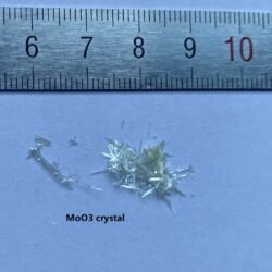
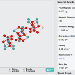
α-MoO₃ Crystals
Price range: £459.99 through £499.99 -
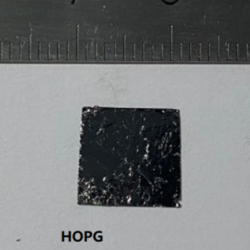
HOPG
£479.99 -
FeBr₃ Crystals
Price range: £469.99 through £499.99 -
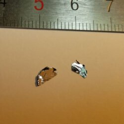
MoTe₂ Crystals (2H phase)
Price range: £499.99 through £569.99 -
WSeTe Crystals
Price range: £599.99 through £899.99 -
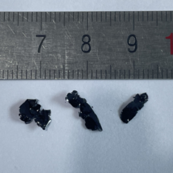
RuCl₃ Crystals
Price range: £499.99 through £899.99 -
VS₂ Crystals
Price range: £499.99 through £569.99 -
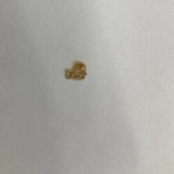
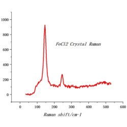
FeCl₂ Crystals
Price range: £499.99 through £569.99 -
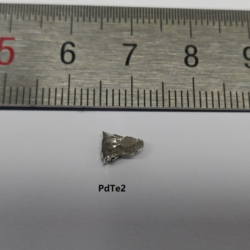
PdTe₂ Crystals
£499.99