
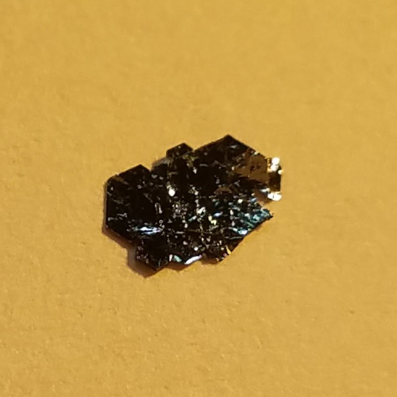
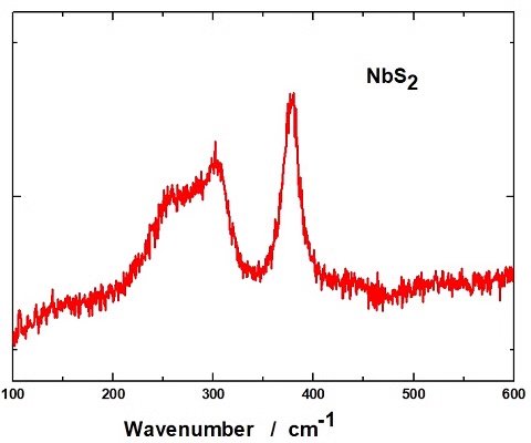
NbS₂ (3R Phase) Crystals
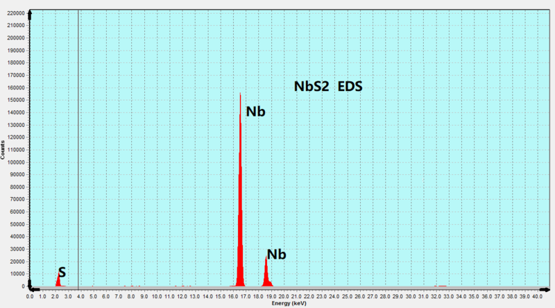
NbS₂ (Niobium Disulfide, 3R Phase) is a layered transition metal dichalcogenide (TMD) with a van der Waals structure. It is well-known for its unique superconducting, electronic, and optical properties, making it a valuable material for applications in nanoelectronics, spintronics, superconductivity research, and 2D material studies. Our NbS₂ (3R) crystals are synthesized using the Chemical Vapor Transport (CVT) method, ensuring high purity, superior crystallinity, and well-controlled stoichiometry.
Sample Size Options:
Crystals larger than 10 mm²
Crystals larger than 25 mm²
Crystals larger than 100 mm²
Material Properties:
Layered van der Waals Structure: Facilitates easy exfoliation into monolayers or few-layer nanosheets for 2D materials research.
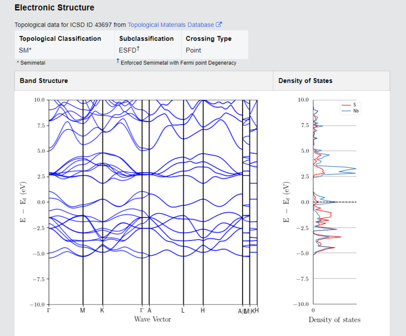
Superconducting Behavior: NbS₂ exhibits superconductivity at low temperatures, making it a promising material for quantum applications. Charge Density Wave (CDW) Effects: The material shows CDW transitions, which are useful for advanced condensed matter research.
Strong Spin-Orbit Coupling: Suitable for spintronic applications due to its interaction with spin-polarized states. Excellent Chemical and Thermal Stability: Maintains stability under ambient conditions, enabling reliable performance in various device applications.
Crystal Structure:
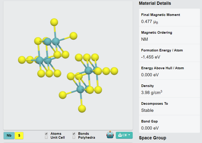
Type: 3R phase (rhombohedral) layered structure
Features: High crystallinity with uniform, defect-free layers, ideal for thin-film fabrication and nanoscale device integration.
Degree of Exfoliation:
Ease of Use: Easily exfoliated into monolayers or few-layer nanosheets for advanced materials research and heterostructure fabrication.
Other Characteristics:
Anisotropic Electronic Properties: Exhibits direction-dependent charge transport behavior. Potential for Superconducting Devices: Ideal for low-temperature quantum and superconducting circuits. Metallic Conductivity in Few Layers: Layer-dependent tunability of electronic properties.
Applications:
Superconductivity Research:
Ideal for studying charge density wave effects and superconducting behavior in 2D systems. Nanoelectronics:
High-performance material for transistors, electronic circuits, and quantum devices. Spintronics:
Useful for exploring spin-orbit coupling and spin-related quantum phenomena.
2D Material Studies:
Excellent for exfoliation into monolayers and integration into van der Waals heterostructures. Energy Storage & Catalysis:
Potential applications in battery electrodes, hydrogen evolution reactions (HER), and catalytic processes. Synthesis Method:
Chemical Vapor Transport (CVT): Ensures high-quality crystals with excellent purity, uniform thickness, and high structural integrity.
| Option 1 | > 10 mm², > 100 mm², > 25 mm² |
|---|
Related products
-
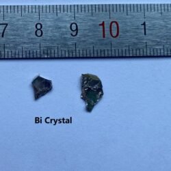
Bi Crystals
£499.99 -

BiI₃ Crystals
Price range: £499.99 through £899.99 -
FeCl₃ Crystals
Price range: £499.99 through £899.99 -
VS₂ Crystals
Price range: £499.99 through £569.99 -
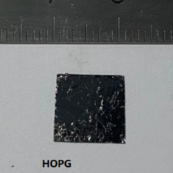
HOPG
£479.99 -
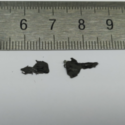
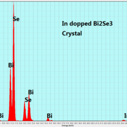
InBiSe₃ Crystals
Price range: £499.99 through £899.99 -
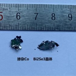
Co-Doped Bi₂Se₃ Crystals
£499.99 -
NiI₃ Crystals
Price range: £499.99 through £899.99 -
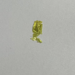
GaS Crystals
Price range: £499.99 through £569.99 -
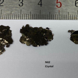
NiI₂ Crystals
Price range: £499.99 through £998.99