
Molybdenum Disulfide (MoS₂)
£377.99
Dispatch normally within 1 business day; carrier transit normally 6–8 business days (7–9 business days in total). See Shipping Policy and Returns Policy.
For research and laboratory use only. Not for medical, diagnostic or household use.
Molybdenum Disulfide (MoS₂)
CAS Number: 1317-33-5
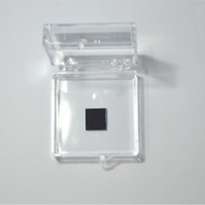
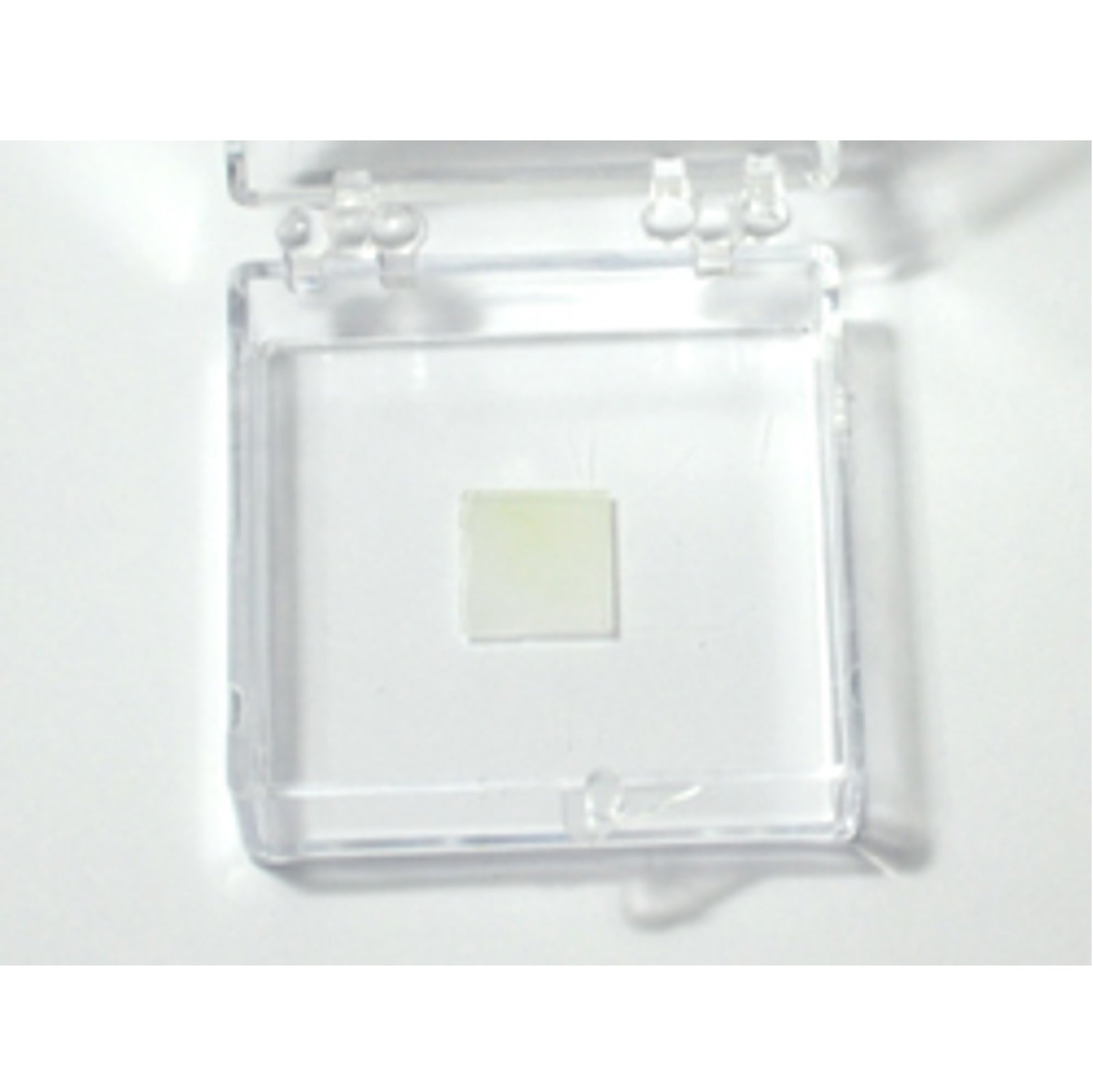
Substrate Size: 1 cm x 1 cm
Preparation Method: Chemical Vapor Deposition (CVD)
Substrate Options:
MoS₂ films are directly grown on SiO₂/Si or sapphire substrates. Custom transfer to other substrates is available upon request-please contact us at sales@nanostoreltd.com for assistance.
Fundamental Properties:
Undoped molybdenum disulfide (MoS₂) is a layered n-type semiconductor belonging to the family of transition metal dichalcogenides. In its monolayer form, MoS₂ has a direct bandgap of approximately 1.85 eV, making it used for optoelectronic applications. In bulk form, MoS₂ exhibits an indirect bandgap of 1.23 eV. The bandgap of multilayer MoS₂ lies between these two values, gradually transitioning from direct to indirect as the number of layers increases.
Applications:
MoS₂ thin films are used in optoelectronic devices, microelectronics, biosensors, and chemical sensors.
References:
1. Gao, M.-R., Liang, J.-X., Zheng, Y.-R., Xu, Y.-F., Jiang, J., Gao, Q., Li, J., & Yu, S.-H. (2015). An efficient molybdenum disulfide/cobalt diselenide hybrid catalyst for electrochemical hydrogen generation. Nature Communications, 6, 5982. https://doi.org/10.1038/ncomms6982
2. Radisavljevic, B., Radenovic, A., Brivio, J., Giacometti, I. V., & Kis, A. (2011). Single-layer MoS₂ transistors. Nature Nanotechnology, 6(3), 147-150. https://doi.org/10.1038/nnano.2010.279
3. Wang, Q. H., Kalantar-Zadeh, K., Kis, A., Coleman, J. N., & Strano, M. S. (2012). Electronics and optoelectronics of two-dimensional transition metal dichalcogenides. Nature Nanotechnology, 7(11), 699-712. https://doi.org/10.1038/nnano.2012.193
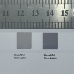
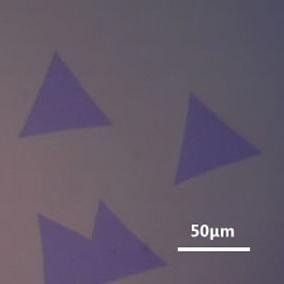
For the 1 cm x 1 cm MoS₂ format on sapphire or SiO₂/Si, the continuous monolayer and multilayer options describe sheet-like films, while the monolayer-triangle option describes triangular regions. Within each MoS₂ layer, a plane of molybdenum atoms lies between sulfur atomic planes.
During CVD, vapour-phase species react at the substrate surface to form MoS₂. Sapphire provides a rigid, electrically insulating support; its single-side- and double-side-polished options distinguish which substrate faces are polished. On SiO₂/Si, the film contacts an insulating oxide surface supported by silicon.
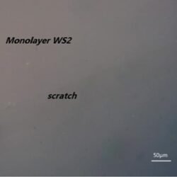
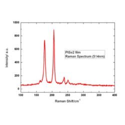
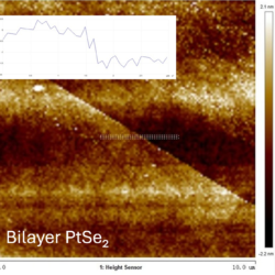
Raman spectroscopy and photoluminescence are typically used to check the vibrational and optical properties of MoS₂ films, whereas optical microscopy and AFM are typically used to examine film morphology and surface topography.
Typical properties of the bulk material (literature values)
| Chemical formula | MoS₂ |
|---|
Source: PubChem (U.S. National Library of Medicine). Reference values for the bulk substance, not test results of a specific lot.
| Option 1 | Continuous Monolayer Film, Continuous Multilayer Film, Monolayer Triangles |
|---|---|
| Option 2 | Sapphire (Double-Side Polished), Sapphire (Single-Side Polished), SiO₂/Si (300 nm SiO₂ Layer) |