

Platinum Diselenide (PtSe₂)
£429.99
Dispatch normally within 1 business day; carrier transit normally 6–8 business days (7–9 business days in total). See Shipping Policy and Returns Policy.
For research and laboratory use only. Not for medical, diagnostic or household use.
Platinum Diselenide (PtSe₂)
CAS Number: 12038-26-5
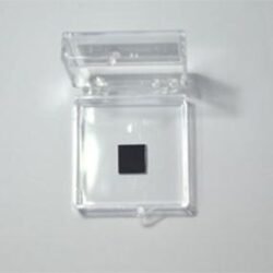
Substrate Size: 1 cm x 1 cm
Preparation Method: Chemical Vapor Deposition (CVD)
Substrate Options:
PtSe₂ films are directly grown on sapphire substrates. Custom transfer to other substrates is available upon request-please contact us at sales@nanostoreltd.com for assistance.
Fundamental Properties:
Platinum diselenide (PtSe₂) is a layered transition metal dichalcogenide (TMD) with a semimetallic character in its bulk form. Unlike many other TMDs, PtSe₂ exhibits a transition from semimetallic to semiconducting behavior as it transitions from bulk to monolayer. Monolayer PtSe₂ has an indirect bandgap of approximately 1.2 eV, and it is used in electronics and optoelectronics. PtSe₂ also possesses environmental stability, carrier mobility, and spin-orbit coupling, supporting applications. Its catalytic activity further supports its use in energy and chemical applications.
Applications:
Electronics: PtSe₂’s semiconducting properties in its monolayer form and semimetallic behavior in bulk support use in field-effect transistors (FETs) and other electronic devices.
Optoelectronics: The tunable bandgap of PtSe₂ allows for its integration into photodetectors, solar cells, and light sensors. Energy Storage and Catalysis: PtSe₂ demonstrates catalytic activity for hydrogen evolution reactions (HER) and is a material for energy storage devices, including supercapacitors and batteries.
Sensors: PtSe₂-based gas and chemical sensors exhibit sensitivity and selectivity, owing to its electronic properties.
Quantum Technologies: Its spin-orbit coupling supports spintronic applications and other quantum technologies.
Bilayer through seven-layer PtSe₂ options are offered in the listed 1 cm x 1 cm sapphire format, with single-side-polished or double-side-polished substrate finishes. The sapphire provides a rigid, electrically insulating support beneath the film.
Within each PtSe₂ sheet, a platinum plane lies between selenium planes, while van der Waals interactions bind adjacent sheets. CVD involves vapour-phase reactants participating in chemical reactions at a heated surface to form a solid film on the supporting substrate.
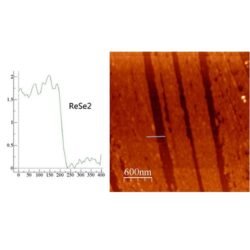
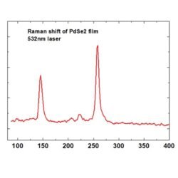
Raman spectroscopy is typically used to examine in-plane and out-of-plane lattice vibrations in PtSe₂. AFM is typically used to assess the surface topography of sapphire-supported PtSe₂ films. XPS is typically used to evaluate the chemical states of platinum and selenium near the film surface.
Typical properties of the bulk material (literature values)
| Chemical formula | PtSe₂ |
|---|
Source: PubChem (U.S. National Library of Medicine). Reference values for the bulk substance, not test results of a specific lot.
| Option 1 | Bilayer, Five Layers, Four Layers, Seven Layers, Six Layers, Trilayer |
|---|---|
| Option 2 | Sapphire (Double-Side Polished), Sapphire (Single-Side Polished) |