
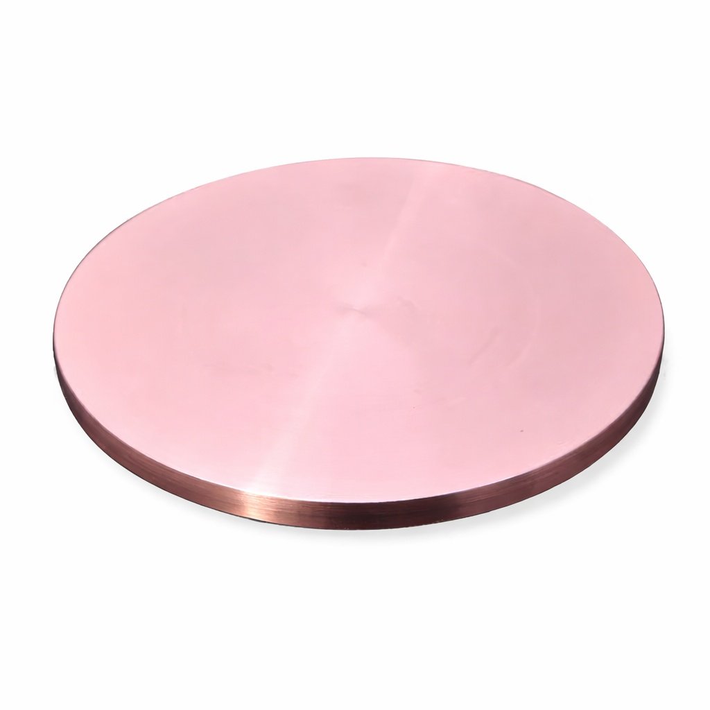
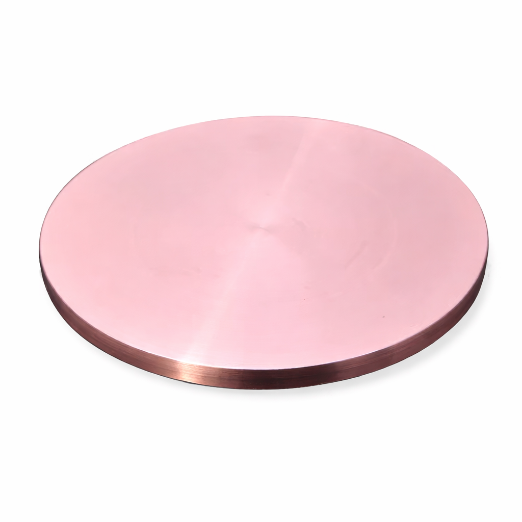
Copper (Cu) Sputtering Target, 99.99% (4N) Purity, Circular
Price range: £105.99 through £142.99
Dispatch normally within 1 business day; carrier transit normally 6–8 business days (7–9 business days in total). See Shipping Policy and Returns Policy.
For research and laboratory use only. Not for medical, diagnostic or household use.
Copper (Cu) Sputtering Target, 99.99% (4N) Purity, Circular
Nanostore’s Copper (Cu) Sputtering Target is a high-purity circular disc manufactured for magnetron sputtering deposition of copper thin films. The target is produced from 99.99% (4N) purity copper feedstock through controlled large-deformation processing to achieve a fine, uniform grain structure that promotes consistent sputter erosion rates, low particle generation, and repeatable film composition across the target lifetime. Copper thin films deposited from this target exhibit high electrical and thermal conductivity, high electromigration resistance, and fit with standard semiconductor interconnect and barrier layer processes. Available in 2 inch and 3 inch diameter configurations with multiple thickness options to match research-scale and production-scale magnetron cathode geometries. Custom sizes, purities (up to 99.9999%), and backing plate bonding services are available upon request.
MATERIAL SPECIFICATIONS:
Material: copper (Cu)
CAS number: 7440-50-8
Purity: 99.99% (4N)
Shape: circular disc
Available sizes: 2 inch dia × 3 mm thick (φ50.8 × 3 mm); 3 inch dia × 3 mm thick (φ76.2 × 3 mm); 3 inch dia × 6 mm thick (φ76.2 × 6 mm)
Appearance: metallic reddish-pink, polished surface
Melting point: 1,085 °C (1,985 °F)
Density: 8.96 g/cm³
Sputtering method: DC magnetron sputtering, RF magnetron sputtering
Maximum power density: consult cathode manufacturer specifications
COMMON APPLICATIONS: Magnetron sputter deposition of copper thin films for semiconductor interconnect metallization and diffusion barrier seed layers; electrode fabrication in MEMS, sensors, and microelectronic devices; deposition of conductive layers in solar cell and photovoltaic research; copper seed layers for electroplating processes; optical and decorative coatings; research-grade thin film studies in materials science, physics, and electrical engineering laboratories.
USAGE NOTES: Mount target onto the magnetron cathode with the polished face oriented toward the substrate. Ensure uniform thermal contact between the target and the cathode cooling plate; thermal transfer paste or indium bonding may be required depending on cathode design. For DC magnetron sputtering, a typical starting power density is 5–10 W/cm²; increase gradually while monitoring plasma behavior and target temperature. Use high-purity argon (99.999%) as the sputtering gas. Recommended base pressure before deposition: ≤5 × 10⁻⁶ Torr. Store in the original sealed packaging in a clean, dry environment to prevent surface oxidation. If oxidation occurs, the target surface can be pre-sputtered to remove the oxide layer before film deposition. Custom dimensions, higher purities (99.999% and 99.9999%), and indium bonding to oxygen-free copper backing plates are available upon request.
Specifications
| Material | copper (Cu) |
|---|---|
| Purity | 99.99% (4N) |
| Shape | circular disc |
| Available sizes | 2 inch dia × 3 mm thick (φ50.8 × 3 mm); 3 inch dia × 3 mm thick (φ76.2 × 3 mm); 3 inch dia × 6 mm thick (φ76.2 × 6 mm) |
| CAS number | 7440-50-8 |
| Appearance | metallic reddish-pink, polished surface |
| Density | 8.96 g/cm³ |
| Melting point | 1,085 °C (1,985 °F) |
Typical properties of the bulk material (literature values)
| Chemical formula | Cu |
|---|---|
| Molar mass | 63.55 g/mol |
| Boiling point | 2835 K |
Source: PubChem (U.S. National Library of Medicine). Reference values for the bulk substance, not test results of a specific lot.
| Option 1 | 2 inch dia × 3 mm thick (φ50.8 × 3 mm), 3 inch dia × 3 mm thick (φ76.2 × 3 mm), 3 inch dia × 6 mm thick (φ76.2 × 6 mm) |
|---|
Related products
-
Niobium Nitride (NbN) Sputtering Target, 99.9% (3N) Purity, Circular
SKU: NBN-TAR-3N-CIRCPrice range: £770.99 through £1,713.99 -
Bismuth Iron Garnet (Bi₃Fe₅O₁₂) Sputtering Target, 99.99% (4N) Purity, Circular (Price Upon Request)
SKU: BI3FE5O12-TAR-4N-CIRCPrice upon request -

Graphite (C) Sputtering Target, 99.999% Purity, Circular
SKU: C-TAR-5N-GRAPHITE-CIRCPrice range: £129.99 through £283.99 -

Lead Telluride (PbTe) Sputtering Target, 99.999% (5N) Purity, Circular (Price Upon Request)
SKU: PBTE-TAR-5N-CIRCPrice upon request