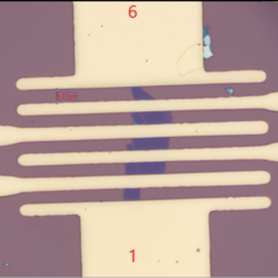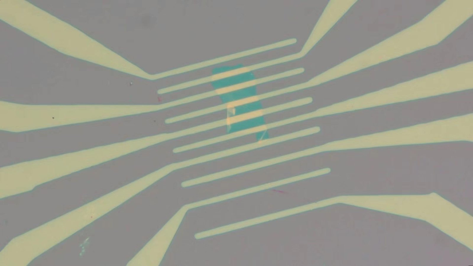
WS₂ FET Device
Device Specifications:
Packaging: Single device (1 unit per package)
Device Dimensions: 1 cm x 1 cm
Substrate: SiO₂/Si (Silicon with 300 nm SiO₂ layer)
Device Structure:
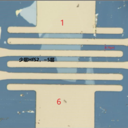
SiO₂/Si Substrate / WS₂ Channel / Au or Cr+Au Electrodes
Device Description & Features:
High-Performance 2D Semiconductor: Tungsten disulfide (WS₂) is a layered transition metal dichalcogenide (TMD) with a direct bandgap (~2.0 eV in monolayer form) and an indirect bandgap in multilayer form, making it ideal for high-performance electronic and optoelectronic applications. Back-Gated FET Configuration: The SiO₂/Si substrate serves as a global back-gate, enabling efficient electrostatic control over the WS₂ channel. Stable n-Type or Ambipolar Conductivity: WS₂ exhibits high electron mobility and can demonstrate ambipolar transport under certain gating conditions. Mechanically Exfoliated or CVD-Grown WS₂: Ensures high crystal quality, minimal defects, and superior charge transport.
Ohmic Contact Engineering: Au or Cr+Au electrodes provide low-resistance metal contacts, optimizing carrier injection.
Applications:
High-Performance Field-Effect Transistors (FETs):
WS₂ FETs exhibit high electron mobility, strong gate tunability, and a high on/off ratio, making them suitable for next-generation nanoelectronics. Flexible and Transparent Electronics:
Ideal for wearable electronics, transparent circuits, and flexible transistors due to WS₂’s mechanical flexibility and optical transparency. Optoelectronic & Photodetector
Applications:
The direct bandgap of monolayer WS₂ makes it ideal for photodetectors, LEDs, and photovoltaic applications. Spintronics & Quantum Transport:
The strong spin-orbit coupling in WS₂ enables potential applications in spintronic and quantum devices.
| Option 1 | Few-layer (~5 layers), Multilayer (~10 layers) |
|---|
Related products
-


-

Monolayer 2H-MoTe₂ FET Device
£599.99 -
-
-
WSe₂ FET Device
£599.99 -
MoS₂ FET Device
£599.99 -
-
-
Graphene FET Device
£599.99 -