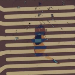
Mechanically Exfoliated Monolayer Graphene FET
£599.99
Flat rate shipping £15
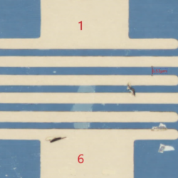
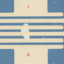
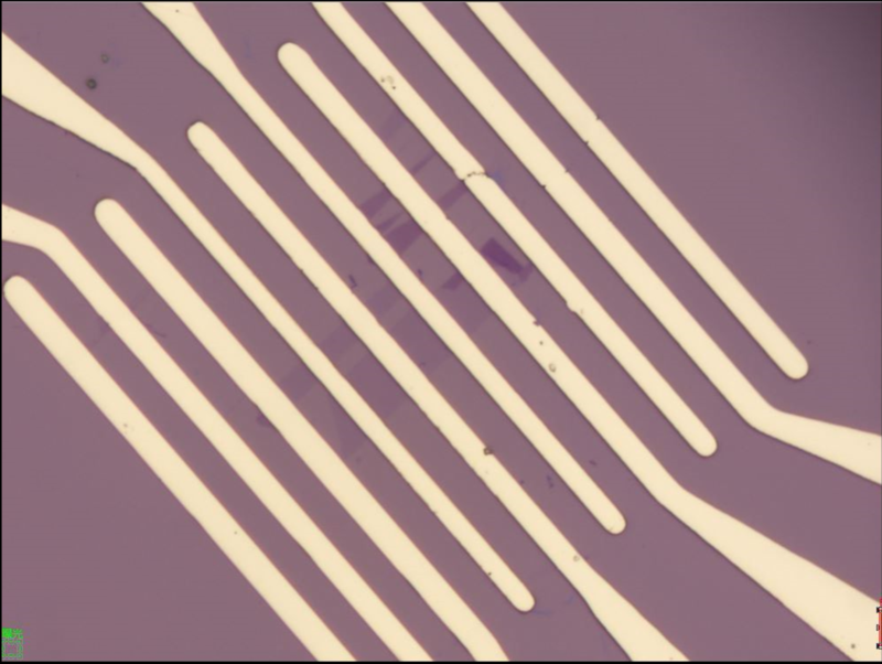
Mechanically Exfoliated Monolayer Graphene FET
Device Structure:
Highly Doped Conductive Si Substrate / 300 nm SiO₂ Layer / Monolayer Graphene / Cr+Au Electrodes
Device Specifications:
Graphene Thickness: Monolayer
Electrode Material: Cr+Au
Gate Dielectric: 300 nm SiO₂
For specific device modifications, please contact us.
Device Description & Features:
Ultra-High Carrier Mobility: Graphene exhibits ballistic transport, extremely high carrier mobility (>10,000 cm²/V-s), and a linear band structure, making it an ideal high-speed transistor material. Back-Gated FET Configuration: The SiO₂/Si back-gate structure provides efficient electrostatic control, enabling low-power operation and high switching speeds.
Mechanically Exfoliated Monolayer Graphene: Preserves intrinsic properties, ensuring low defect density, minimal scattering, and superior electrical performance.
Ohmic Metal Contacts: Cr+Au electrodes provide low-resistance contacts, optimizing charge injection and transport.
Ambipolar Conductivity: Graphene allows for electron and hole conduction, making it suitable for reconfigurable electronic circuits.
Applications:
High-Performance Field-Effect Transistors (FETs):
Graphene FETs demonstrate ultrafast switching, high-frequency operation, and excellent gate tunability for next-generation nanoelectronics. Flexible and Transparent Electronics:
Graphene’s mechanical flexibility and optical transparency (~97.7%) make it ideal for flexible, stretchable, and transparent electronic devices. Optoelectronic & THz
Applications:
The broadband absorption and ultrafast response of graphene enable photodetectors, optical modulators, and THz applications. Quantum Transport & Spintronics:
Graphene’s Dirac-like electronic structure allows potential applications in quantum computing, spintronics, and valleytronics.
| Option 1 | Few-layer (~5 layers), Multilayer (~10 layers) |
|---|
Related products
-

Monolayer 2H-MoTe₂ FET Device
£599.99 -
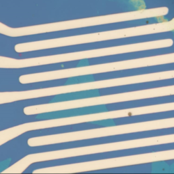
MoS₂ FET Device
£599.99 -


-
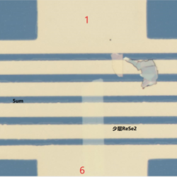
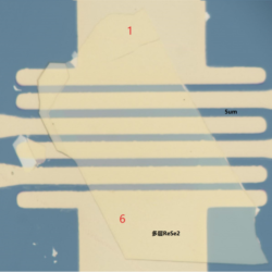
-
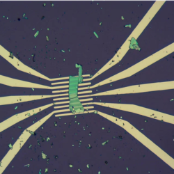
Multilayer ReS₂/PdSe₂ FET Device
£599.99 -
-
-
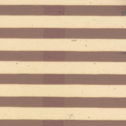
Graphene FET Device
£599.99 -
-