
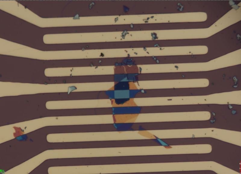
Black Phosphorus/ReSe₂ FET Device
Heterojunction FET Device
Device Structure:
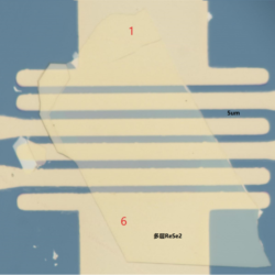
Conductive Si Substrate / 300 nm SiO₂ Layer / 5 µm Gold Electrode Array / ReSe₂ / Black Phosphorus
Device Description & Features:
2D van der Waals Heterojunction: The combination of anisotropic black phosphorus (BP) and ReSe₂ forms a type-II band-aligned heterostructure, enabling efficient charge separation and enhanced carrier transport. Layer-Dependent Bandgap Engineering:
Black Phosphorus (BP): A layer-tunable direct bandgap (~0.3 eV for bulk, ~1.5 eV for monolayer) offering high mobility and strong anisotropy.
ReSe₂: A low-symmetry TMD with an anisotropic band structure (~1.3 eV direct bandgap in monolayer form), allowing unique transport properties. Back-Gated FET Configuration: The SiO₂/Si back-gate structure provides strong electrostatic control, enabling high on/off current ratio and low-power operation. Gold Electrode Array (5 µm spacing): Facilitates uniform carrier injection while preserving intrinsic 2D transport properties.
Applications:
High-Performance Field-Effect Transistors (FETs):
The heterostructure channel enables tunable electronic properties, suitable for next-generation nanoelectronics. Anisotropic Charge Transport & Directional Electronics:
The layered anisotropic nature of BP and ReSe₂ allows studies on directional carrier transport. Optoelectronic & Photodetector
Applications:
The type-II band alignment enhances photogenerated carrier separation, making it ideal for photodetectors and photovoltaics. Neuromorphic & Quantum Computing:
Unique band structure and interlayer coupling effects enable neuromorphic logic and quantum electronic applications.
| Option 1 | Few-layer (~5 layers), Multilayer (~10 layers) |
|---|
Related products
-
-
-
WS₂ FET Device
£599.99 -
MoS₂ FET Device
£599.99 -
Monolayer 2H-MoTe₂ FET Device
£599.99 -
-
-
Graphene FET Device
£599.99 -
-
WSe₂ FET Device
£599.99