

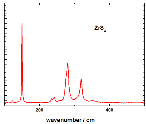
ZrS₃ Crystals
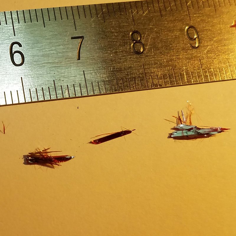
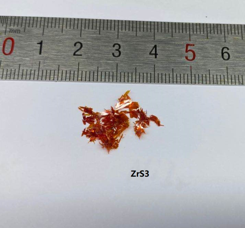
ZrS₃ (Zirconium Trisulfide) is a quasi-one-dimensional (1D) transition metal trichalcogenide (TMT) with highly anisotropic electrical and optical properties. It exhibits a tunable bandgap, strong excitonic effects, and high carrier mobility, making it a promising material for applications in nanoelectronics, optoelectronics, and energy storage. Our ZrS₃ crystals are synthesized using the Chemical Vapor Transport (CVT) method, ensuring high purity, excellent crystallinity, and precise stoichiometry.
Sample Size Options:
Crystals larger than 10 mm²
Crystals larger than 25 mm²
Crystals larger than 100 mm²
Material Properties:
Quasi-1D Layered Structure: Exhibits strong in-plane anisotropy in electrical and optical properties.
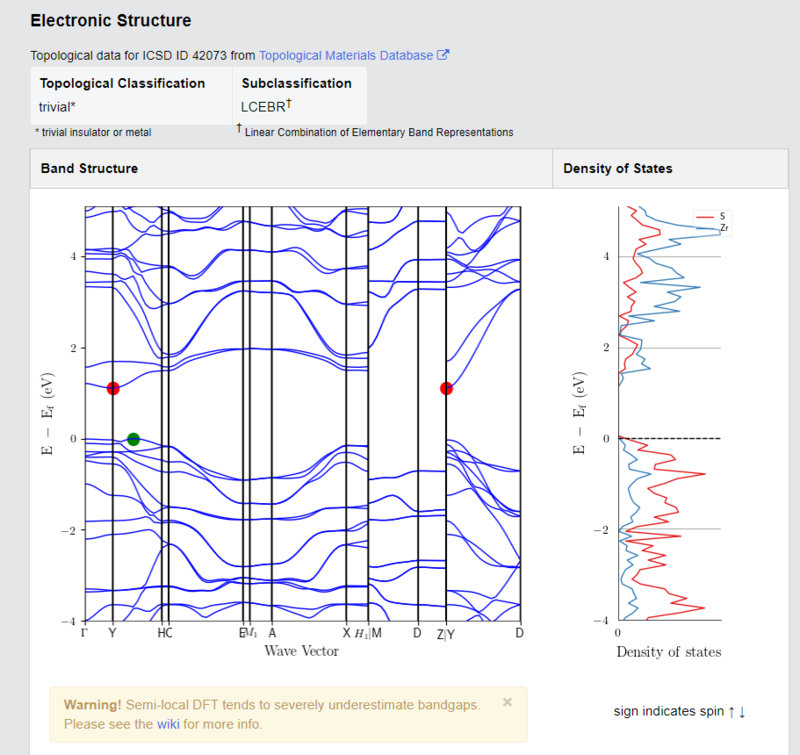
Semiconducting Behavior: Bulk ZrS₃ has an indirect bandgap of ~1.9 eV, which transitions to a direct bandgap in monolayer form (~2.2 eV), making it ideal for optoelectronic applications.
Strong Excitonic Effects: Exhibits pronounced excitonic resonances due to reduced dielectric screening, enhancing optical performance.
Anisotropic Optical Absorption: Strong polarization-dependent optical response, useful for linear dichroism studies.
High Carrier Mobility: Demonstrates excellent charge transport properties, making it suitable for high-speed electronic devices.
Good Environmental Stability: More stable than Mo- and W-based transition metal dichalcogenides (TMDs) under ambient conditions.
Crystal Structure:
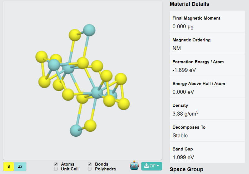
Type: Triclinic layered structure with quasi-1D properties
Features: High crystallinity with uniform, defect-free layers, ideal for thin-film fabrication and nanoscale device applications.
Degree of Exfoliation:
Ease of Use: Easily exfoliated into few-layer nanosheets for advanced materials research and heterostructure fabrication.
Other Characteristics:
Anisotropic Transport Properties: Exhibits direction-dependent charge transport, suitable for novel electronic and quantum devices. Potential for Excitonic Devices: Strong electron-hole interactions make it valuable for next-generation optoelectronic applications. Tunable Optical & Electronic Properties: Bandgap and charge transport can be modified via layer thickness and strain engineering.
Applications:
Optoelectronics & Photodetectors:
Ideal for polarization-sensitive photodetectors and infrared light sensors.
Nanoelectronics: Suitable for high-speed transistors, thin-film semiconductors, and next-generation electronic devices. Energy Storage & Conversion:
Investigated for applications in lithium-ion and sodium-ion batteries due to its good electrochemical performance.
2D Material Studies:
Perfect for exfoliation into monolayers and integration into van der Waals heterostructures. Quantum Materials Research:
Enables exploration of excitonic interactions, anisotropic quantum transport, and valleytronic effects. Synthesis Method:
Chemical Vapor Transport (CVT): Ensures high-quality crystals with excellent purity, uniform thickness, and high structural integrity.
| Option 1 | > 10 mm², > 100 mm², > 25 mm² |
|---|
Related products
-

MoTe₂ Crystals (2H phase)
Price range: £499.99 through £569.99 -
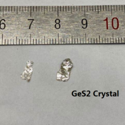

GeS₂ Crystals
Price range: £499.99 through £599.99 -
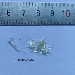
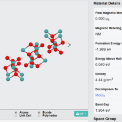
α-MoO₃ Crystals
Price range: £459.99 through £499.99 -
NiI₃ Crystals
Price range: £499.99 through £899.99 -

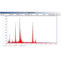
Co₃Sn₂S₂ Crystals
£599.99 -
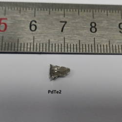
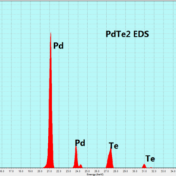
PdTe₂ Crystals
£499.99 -
HOPG
£479.99 -

GeS Crystals
Price range: £499.99 through £549.99 -
CrBr₃ Crystals
£499.99 -
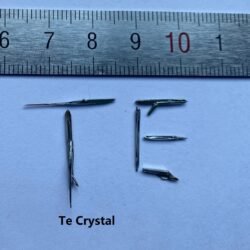
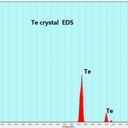
Te Crystals
£499.99