
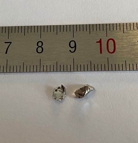
SbTe Crystals
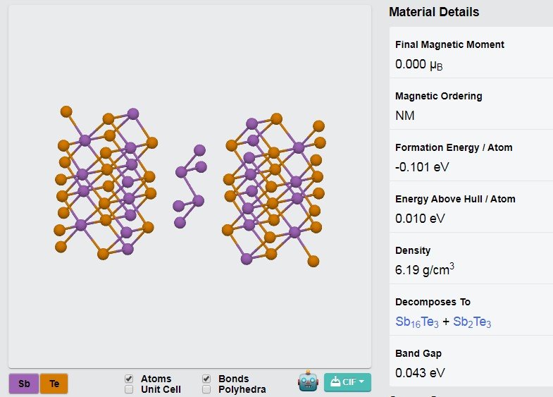
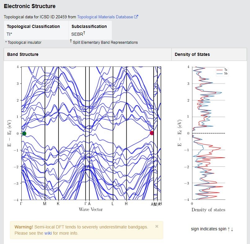
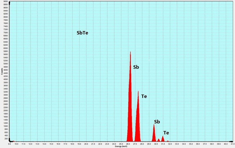
SbTe is a layered thermoelectric material with a van der Waals structure, known for its high thermoelectric and electronic properties. Its high Seebeck coefficient, low thermal conductivity, and robust surface states make it an ideal material for thermoelectric energy conversion, quantum materials research, and advanced spintronic applications. Our SbTe crystals are synthesized using the Chemical Vapor Transport (CVT) method, ensuring high purity, precise stoichiometry, and high crystallinity.
Sample Size Options:
Crystals larger than 10 mm²
Crystals larger than 25 mm²
Material Properties:
Layered van der Waals Structure: Facilitates exfoliation into thin layers for 2D material studies.
Thermoelectric Performance: High efficiency with a large Seebeck coefficient and low thermal conductivity.
Electronic Conductivity: Excellent carrier mobility for electronic and energy applications.
Optical Properties: Strong absorption in the visible-to-infrared range.
Crystal Structure:
Type: Rhombohedral layered structure
Features: Cleavable layers, suitable for thin-film fabrication and nanoscale research.
Degree of Exfoliation:
Ease of Use: Readily exfoliates into monolayers or few-layer sheets for advanced research.
Other Characteristics:
Thermoelectric Efficiency: Suitable for power generation and thermal management.
Quantum Properties: Promising for studying low-dimensional electronic and thermoelectric phenomena. Spintronics
Applications: Ideal for exploring spin-related phenomena and spintronic devices.
Applications:
Thermoelectric Devices:
Ideal for energy harvesting, cooling systems, and thermal-to-electric conversion. Quantum Materials Research:
Enables exploration of topological states and low-dimensional transport properties. Spintronics:
Suitable for spintronic devices and investigating spin-orbit coupling.
2D Material Studies:
Perfect for exfoliation into thin layers and integration with van der Waals heterostructures. Optoelectronics:
Suitable for photodetectors and other optoelectronic devices.
| Option 1 | > 10 mm², > 25 mm² |
|---|
Related products
-
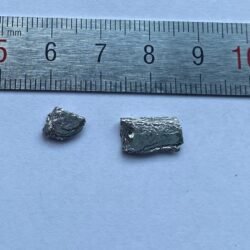
Ni₂Bi₂Te₅ Crystals
Price range: £499.99 through £569.99 -
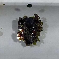
CrBr₃ Crystals
£499.99 -
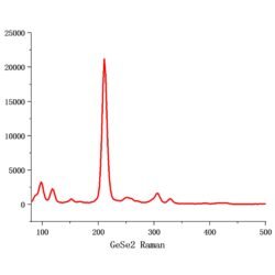
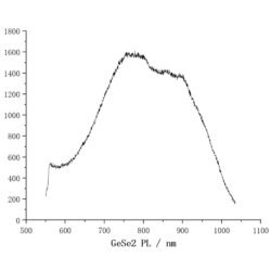
GeSe₂ Crystals
Price range: £499.99 through £569.99 -
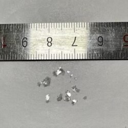
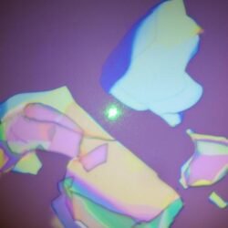
BiOCl Crystals
Price range: £499.99 through £569.99 -
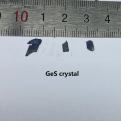
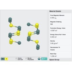
GeS Crystals
Price range: £499.99 through £549.99 -
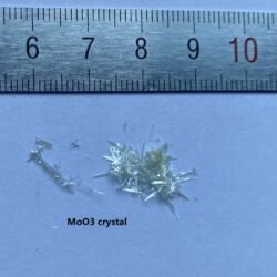
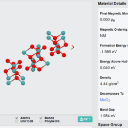
α-MoO₃ Crystals
Price range: £459.99 through £499.99 -
FeBr₃ Crystals
Price range: £469.99 through £499.99 -
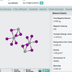
VI₃ Crystals
Price range: £499.99 through £599.99 -
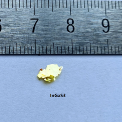
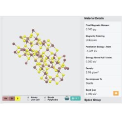
InGaS₃ Crystals
£499.99 -
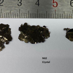
NiI₂ Crystals
Price range: £499.99 through £998.99