
In₂P₃S₉ Crystals
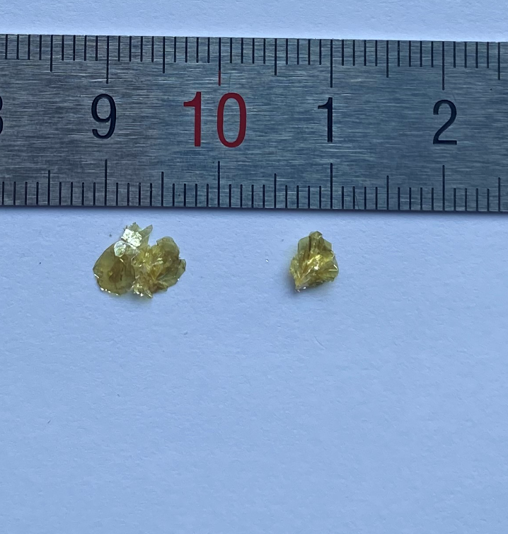
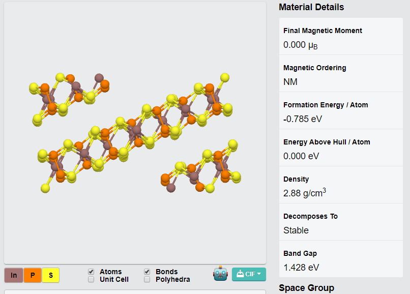
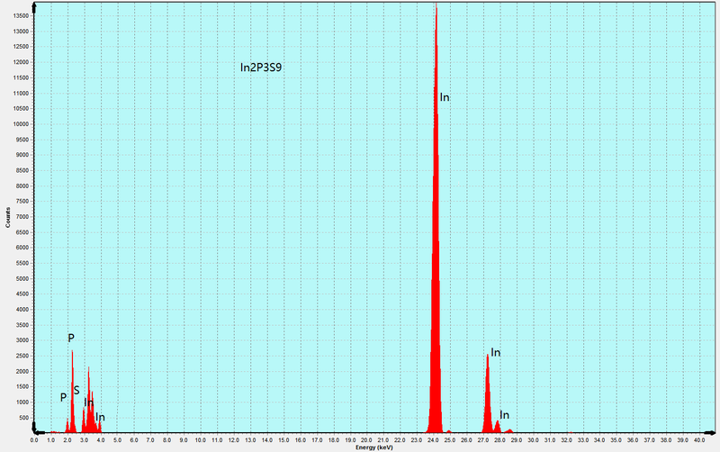
In₂P₃S₉ is a layered thiophosphate material with a van der Waals structure, exhibiting unique semiconducting and optical properties. Its high optical absorption, tunable bandgap, and excellent stability make it a promising material for optoelectronics, energy storage, and advanced 2D material research. Our In₂P₃S₉ crystals are synthesized using the Chemical Vapor Transport (CVT) method to ensure high purity, high crystallinity, and reliable performance for cutting-edge research applications.
Sample Size Options:
Crystals larger than 10 mm²
Crystals larger than 25 mm²
Crystals larger than 100 mm²
Material Properties:
Layered van der Waals Structure: Facilitates exfoliation into thin layers for 2D material research.
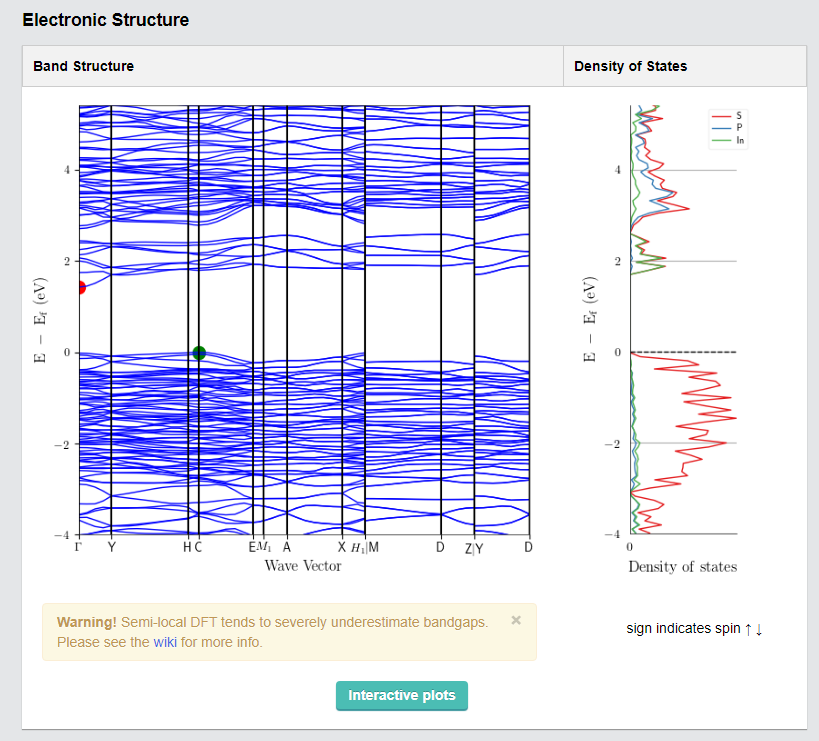
Semiconducting Behavior: Features a tunable bandgap suitable for optoelectronic applications.
High Optical Absorption: Strong absorption in the visible-to-near-infrared range.
Environmental Stability: Maintains stability under inert storage conditions.
Crystal Structure:
Type: Layered triclinic structure
Features: Cleavable into thin sheets, ideal for nanoscale research and device fabrication.
Degree of Exfoliation:
Ease of Use: Readily exfoliates into monolayers or few-layer sheets for advanced applications.
Other Characteristics:
Optoelectronic Potential: Strong photoluminescence and absorption for photonic devices. Energy
Applications: Promising for thermoelectric and energy conversion technologies.
Anisotropic Properties: Exhibits direction-dependent optical and electronic behavior.
Applications:
Optoelectronics:
Ideal for photodetectors, light-emitting devices, and solar energy harvesting.
2D Material Research:
Suitable for exfoliation into thin layers and integration with van der Waals heterostructures. Energy
Applications:
Promising material for photocatalysis and thermoelectric devices. Quantum Materials Research:
Enables exploration of low-dimensional semiconducting and optoelectronic properties. Sensors:
High sensitivity to environmental stimuli makes it ideal for advanced sensing applications.
| Option 1 | > 10 mm², > 100 mm², > 25 mm² |
|---|
Related products
-
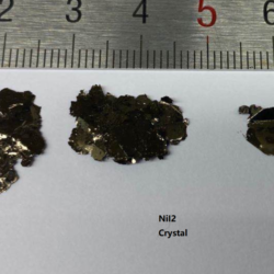
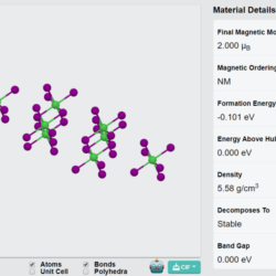
NiI₂ Crystals
Price range: £499.99 through £998.99 -
FeCl₃ Crystals
Price range: £499.99 through £899.99 -
VS₂ Crystals
Price range: £499.99 through £569.99 -

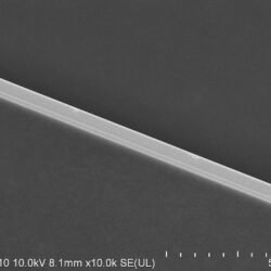
MoTe₂ Crystals (2H phase)
Price range: £499.99 through £569.99 -
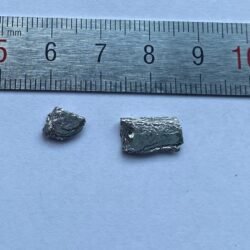
Ni₂Bi₂Te₅ Crystals
Price range: £499.99 through £569.99 -
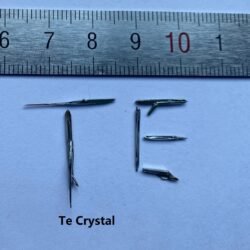
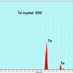
Te Crystals
£499.99 -
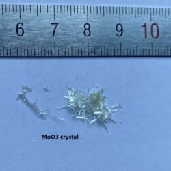
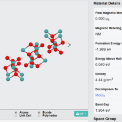
α-MoO₃ Crystals
Price range: £459.99 through £499.99 -
WSeTe Crystals
Price range: £599.99 through £899.99 -
BiI₃ Crystals
Price range: £499.99 through £899.99 -
FeBr₃ Crystals
Price range: £469.99 through £499.99