
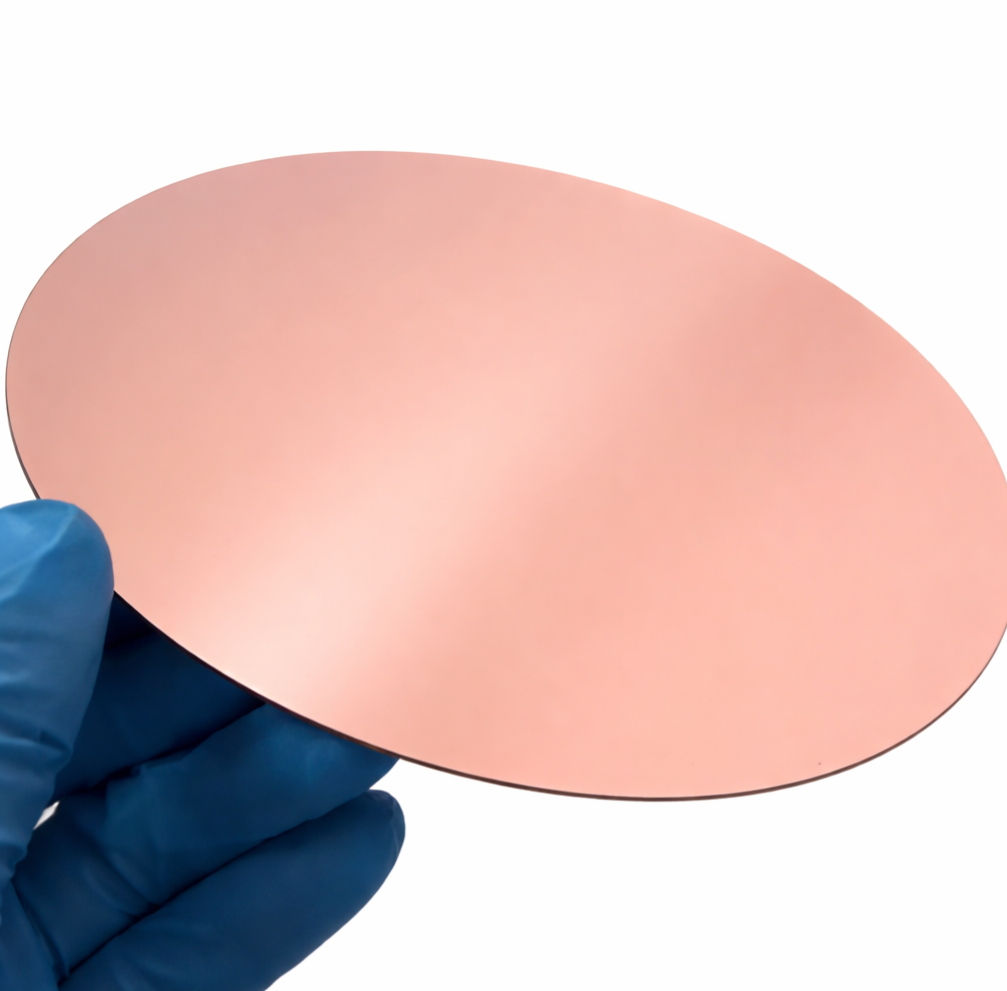
Copper-Coated Silicon Wafers (Cu/Ti on Si (100))
Price range: £142.99 through £478.99
Flat rate shipping £15
Copper-Coated Silicon Wafers (Cu/Ti on Si (100))
Overview
Our copper-coated silicon wafers are fabricated using high-vacuum magnetron sputtering to ensure uniform thickness, strong adhesion, and clean surface morphology suitable for electrochemical research and microfabrication.
A titanium (Ti) adhesion layer is deposited between the silicon substrate and the copper film to enhance interfacial bonding and long-term film stability.
These Cu-coated wafers are widely used in CO₂ reduction research, electrochemical studies, electrode development, seed layer applications, and thin film device fabrication.
Layer Structure
Cu (Copper layer)
Ti (10 nm adhesion layer)
Si (100) substrate
Adhesion Layer
Standard adhesion layer: Ti (10 nm)
This configuration provides reliable adhesion while maintaining good electrical conductivity.
Optional adhesion thickness available upon request.
Recommended Copper Thickness
Standard thickness options:
50 nm–Thin conductive layer / seed layer
100 nm–Recommended (general electrochemical research)
200 nm – Recommended (improved stability & durability)
500 nm – Thick conductive layer
Custom thickness available upon request.
Substrate Specifications
Standard configuration (default)
Orientation: Si (100)
Doping: N-type, 1–10 Ω·cm resistivity
Surface finish: Single-side polished (SSP)
Custom options available upon request:
P-type silicon
Double-side polished (DSP)
Custom resistivity range
Deposition Process
High-vacuum magnetron sputtering
Controlled thickness uniformity
Clean-room compatible handling
Applications
CO₂ reduction reaction (CO2RR)
Electrochemical catalysis research
Electrode platform development
Seed layer for electroplating
Microelectronic interconnect research
MEMS fabrication
Quality & Packaging
Uniform film thickness control
Research-grade surface quality
Protective packaging to minimize oxidation exposure
Custom Orders
We support:
Custom wafer diameter
Custom copper thickness
Custom adhesion thickness
Patterned copper upon request
Contact us for academic pricing and technical consultation.
| Option 1 | 2″ Si | 100 nm Cu, 2″ Si | 200 nm Cu, 2″ Si | 50 nm Cu, 2″ Si | 500 nm Cu, 4″ Si | 100 nm Cu, 4″ Si | 200 nm Cu, 4″ Si | 50 nm Cu, 4″ Si | 500 nm Cu, 6″ Si | 100 nm Cu, 6″ Si | 200 nm Cu, 6″ Si | 50 nm Cu, 6″ Si | 500 nm Cu, 8″ Si | 100 nm Cu, 8″ Si | 200 nm Cu |
|---|
Related products
-
Copper-Coated Silicon Substrates (Cu/Ti on Si (100))
Price range: £34.99 through £106.99