
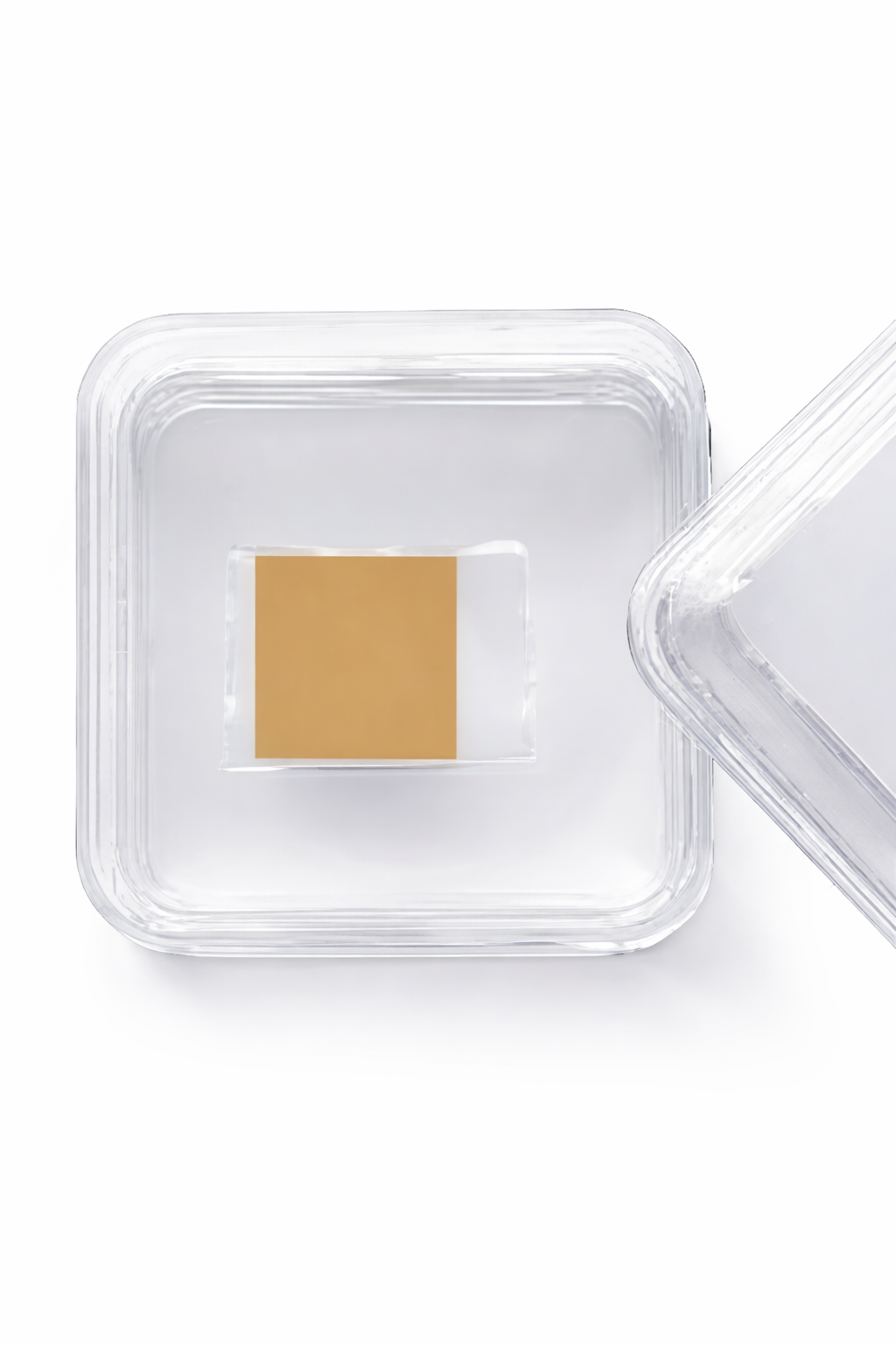
Copper-Coated Silicon Substrates (Cu/Ti on Si (100))
Price range: £34.99 through £106.99
Flat rate shipping £15
Copper-Coated Silicon substrates (Cu/Ti on Si (100))
Overview
Our copper-coated silicon substrates are precision-cut from research-grade Cu thin film wafers fabricated on Si (100) substrates using high-vacuum magnetron sputtering.
A 10 nm titanium (Ti) adhesion layer is deposited between the silicon substrate and the copper film to ensure strong interfacial bonding and stable electrical performance.
These Cu-coated chips are widely used in electrochemical research, CO₂ reduction studies, electrode development, and microfabrication experiments.
Layer Structure
Cu (Copper layer)
Ti (10 nm adhesion layer)
Si (100) substrate
Available Sizes
5 × 5 mm
10 × 10 mm
15 × 15 mm
Copper Thickness Options
100 nm – Recommended for general electrochemical research
200 nm – Recommended for enhanced stability
500 nm – Thick conductive layer for high-current applications
Substrate Specifications
Orientation: Si (100)
Doping: N-type, 1–10 Ω·cm resistivity
Surface finish: Single-side polished (SSP)
Deposition Process
High-vacuum magnetron sputtering
Controlled thickness uniformity
Precision wafer dicing
Clean-room compatible handling
Applications
CO₂ reduction reaction (CO2RR)
Electrochemical catalysis research
Electrode platform development
Electroplating seed layer studies
Microelectronic interconnect research
Quality & Packaging
Uniform film thickness control
Research-grade surface quality
Protective packaging to minimize oxidation exposure
Custom sizes and thicknesses available upon request.
| Option 1 | 10 × 10 mm Si | 100 nm Cu, 10 × 10 mm Si | 200 nm Cu, 10 × 10 mm Si | 500 nm Cu, 15 × 15 mm Si | 100 nm Cu, 15 × 15 mm Si | 200 nm Cu, 5 × 5 mm Si | 100 nm Cu, 5 × 5 mm Si | 200 nm Cu |
|---|
Related products
-
Copper-Coated Silicon Wafers (Cu/Ti on Si (100))
Price range: £142.99 through £478.99