
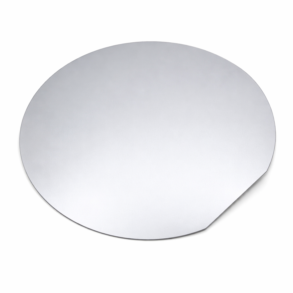
Platinum-Coated Silicon Wafers (Pt/Ti on Si (100))
Price range: £286.99 through £1,318.99
Flat rate shipping £15
Platinum-Coated Silicon Wafers (Pt/Ti on Si (100))
Overview
Our platinum-coated silicon substrates are fabricated using high-vacuum magnetron sputtering to ensure uniform thickness, excellent adhesion, and high surface quality suitable for advanced research and device fabrication.
A titanium (Ti) adhesion layer is deposited between the silicon substrate and the platinum layer to provide strong interfacial bonding and long-term stability.
These substrates are widely used in electrochemical research, catalysis studies, fuel cell development, and MEMS fabrication.
Layer Structure
Standard structure:
Pt (Platinum layer)
Ti (10 nm adhesion layer)
Si (100) Wafer
Adhesion Layer
Standard adhesion layer: Ti (10 nm)
This configuration is widely used in electrochemical and microfabrication applications due to its strong adhesion and stable interface.
Optional: Ti (20 nm)
Recommended for thicker Pt films (>500 nm) or high-temperature applications.
Custom adhesion thickness available upon request.
Platinum Thickness Options
Standard Pt thickness:
50 nm
100 nm
200 nm
500 nm
Custom thickness available upon request.
Substrate Specifications
Standard configuration (default)
Orientation: Si (100)
Doping: N-type, 1–10 Ω·cm resistivity
Surface finish: Single-side polished (SSP)
This configuration is commonly used in laboratory research and device prototyping.
Custom options available
P-type silicon
Double-side polished (DSP)
Custom resistivity
Please contact us for special requirements or bulk orders.
Deposition Process
High-vacuum magnetron sputtering
Controlled deposition ensures good thickness uniformity and reliable electrical performance.
Applications
Electrochemical catalysis (HER, OER, CO2RR)
Fuel cell electrode platforms
Hydrogen evolution studies
High-temperature electrode systems
MEMS sensors
Microelectrode fabrication
Catalytic surface research
Quality & Packaging
Uniform film thickness control
Clean-room compatible handling
Protective packaging to prevent contamination
Research-grade surface quality
Why Choose Our Pt/Ti on Si Substrates?
Research-grade platinum thin films
Optimized Ti adhesion layer
Stable electrochemical performance
Competitive direct-manufacturer pricing
Custom Orders
We support:
Custom wafer size
Custom Pt thickness
Patterned platinum upon request
Contact us for academic pricing and technical consultation.
| Option 1 | 12″ Si | 100 nm Pt, 12″ Si | 50 nm Pt, 2″ Si | 100 nm Pt, 2″ Si | 200 nm Pt, 2″ Si | 50 nm Pt, 2″ Si | 500 nm Pt, 4″ Si | 100 nm Pt, 4″ Si | 200 nm Pt, 4″ Si | 50 nm Pt, 4″ Si | 500 nm Pt, 6″ Si | 100 nm Pt, 6″ Si | 200 nm Pt, 6″ Si | 50 nm Pt, 6″ Si | 500 nm Pt, 8″ Si | 100 nm Pt, 8″ Si | 200 nm Pt, 8″ Si | 50 nm Pt, 8″ Si | 500 nm Pt |
|---|
Related products
-
Platinum-Coated Silicon Substrates (Pt/Ti on Si (100))
Price range: £58.99 through £202.99