
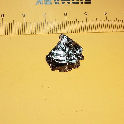
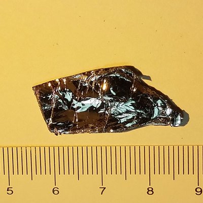
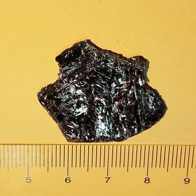
MoS₂ Crystals
MoS₂ is a layered transition metal dichalcogenide (TMD) known for its notable electronic, optical, and catalytic properties. It features a tunable bandgap that transitions from an indirect (~1.2 eV) in bulk to a direct bandgap (~1.8 eV) in monolayer form, making it ideal for applications in optoelectronics, nanoelectronics, and energy conversion. Our medium-area MoS₂ crystals are synthesized using the Chemical Vapor Transport (CVT) method, ensuring high purity, excellent crystallinity, and uniform large-area domains suitable for research and industrial applications.
Sample Size:
Large-Area Crystals (>20 mm x 20 mm)
Medium-Area Crystals (>15 mm x 15 mm)
Small-Area Crystals (>10 mm x 10 mm)
Material Properties:
Layered van der Waals Structure: Facilitates easy exfoliation into monolayers or few-layer sheets for 2D materials research.
Tunable Bandgap: Indirect bandgap (~1.2 eV) in bulk and direct bandgap (~1.8 eV) in monolayer form, suitable for optoelectronic applications.
High Carrier Mobility: Excellent electronic performance, ideal for field-effect transistors (FETs) and nanoelectronic devices.
Strong Photoluminescence: Intense photoluminescence in monolayer form, suitable for light-emitting devices and photodetectors.
High Catalytic Activity: Effective for hydrogen evolution reactions (HER) due to abundant active edge sites.
Crystal Structure:
Type: Hexagonal (2H phase) layered structure
Features: Uniform, defect-free surfaces with excellent crystallinity, perfect for device integration and thin-film fabrication.
Degree of Exfoliation:
Ease of Use: Easily exfoliated into monolayers or few-layer nanosheets for advanced material research, flexible electronics, and heterostructure assembly.
Other Characteristics:
Excellent Mechanical Flexibility: Suitable for flexible and stretchable electronic devices.
Thermal Stability: High thermal and chemical stability under ambient conditions.
Quantum Confinement Effects: Exhibits quantum phenomena at the monolayer level, such as excitonic effects and enhanced optical absorption.
Applications:
Optoelectronics:
Ideal for photodetectors, light-emitting diodes (LEDs), and photovoltaic devices. Nanoelectronics:
High-performance material for transistors, logic devices, and flexible electronic circuits. Catalysis:
Excellent electrocatalyst for hydrogen evolution reactions (HER) and energy storage applications.
2D Material Studies:
Perfect for exfoliation into monolayers and integration into van der Waals heterostructures. Sensors:
High sensitivity for gas detection, biosensing, and chemical sensing applications. Synthesis Method:
Chemical Vapor Transport (CVT): Ensures high-quality crystals with excellent purity, uniform thickness, and high structural integrity.
| Option 1 | >10 mm x 10 mm, >15 mm x 15 mm, >20 mm x 20 mm |
|---|
Related products
-
VS₂ Crystals
Price range: £499.99 through £569.99 -

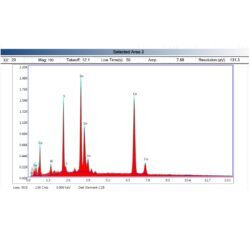
Co₃Sn₂S₂ Crystals
£599.99 -
TiS₃ Crystals
Price range: £469.99 through £899.99 -

WSSe Crystals
Price range: £599.99 through £899.99 -
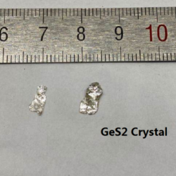
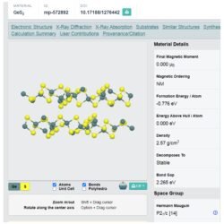
GeS₂ Crystals
Price range: £499.99 through £599.99 -
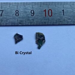
Bi Crystals
£499.99 -
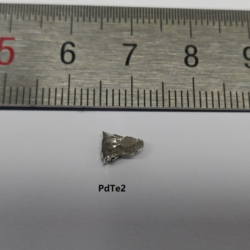
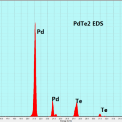
PdTe₂ Crystals
£499.99 -
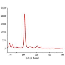
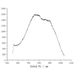
GeSe₂ Crystals
Price range: £499.99 through £569.99 -
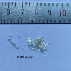
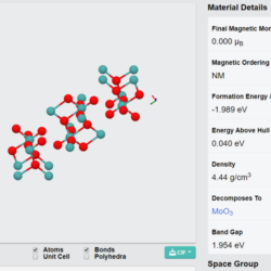
α-MoO₃ Crystals
Price range: £459.99 through £499.99 -
NiI₃ Crystals
Price range: £499.99 through £899.99