
Hexagonal Boron Nitride (h-BN) Transferred onto Sapphire Substrate (1 cm x 1 cm)
£219.99
Flat rate shipping £15
Hexagonal Boron Nitride (h-BN) Transferred onto Sapphire Substrate (1 cm x 1 cm)
CAS Number: 10043-11-5
Preparation Method:
Hexagonal boron nitride (h-BN) films are grown on copper foils using a high-temperature Chemical Vapor Deposition (CVD) process. These high-quality h-BN films are then carefully transferred onto sapphire substrates using a PMMA-assisted wet chemical transfer technique, ensuring uniform films with minimal defects and excellent surface quality. Morphology Options:
Monolayer
Few Layers (<10 layers, ~5 nm) Multilayer (>5 nm)
All options are available at the same price. For specific requirements, please contact us directly.
Substrate Options:
h-BN films are transferred onto sapphire substrates, which provide excellent thermal, optical, and mechanical stability. Custom transfer to other substrate materials is available upon request-please visit our Custom Products page or contact us for assistance.
Fundamental Properties:
Hexagonal boron nitride (h-BN) on sapphire substrates combines the exceptional dielectric, thermal, and chemical stability of h-BN with the robust and optically transparent properties of sapphire. Key properties include:
Chemical Stability: High resistance to oxidation and chemical degradation.
Thermal Stability: Withstands extreme temperatures, complementing sapphire’s high thermal conductivity.
Wide Bandgap: Exceptional dielectric properties with a bandgap of ~5.9 eV.
Optical Transparency: The sapphire substrate is highly transparent in the UV and visible regions, enabling advanced optical applications.
Applications:
Electronics: Ideal as a dielectric layer or insulating substrate for high-performance electronic devices.
Optoelectronics: Suitable for transparent electronics, UV detectors, and other light-emitting devices.
Sensors: A chemically stable insulating material for gas and chemical sensing applications. Energy Applications: Useful as a protective or insulating layer in high-temperature energy storage and conversion devices.
Thermal Management: Ideal for applications requiring thermal insulation or efficient heat dissipation.
| Option 1 | Few Layers (<10 layers, ~5 nm), Monolayer, Multilayer (>5 nm) |
|---|
Related products
-
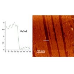
Rhenium Diselenide (ReSe₂)
£429.99 -
-
-
Antimony Telluride (Sb₂Te₃)
£429.99 -
-
Bismuth Selenide (Bi₂Se₃)
£429.99 -
Palladium Diselenide (PdSe₂)
£429.99 -
Tin Sulfide (SnS)
£429.99 -
Nickel Ditelluride (NiTe₂)
£429.99 -
Rhenium Disulfide (ReS₂)
£429.99