
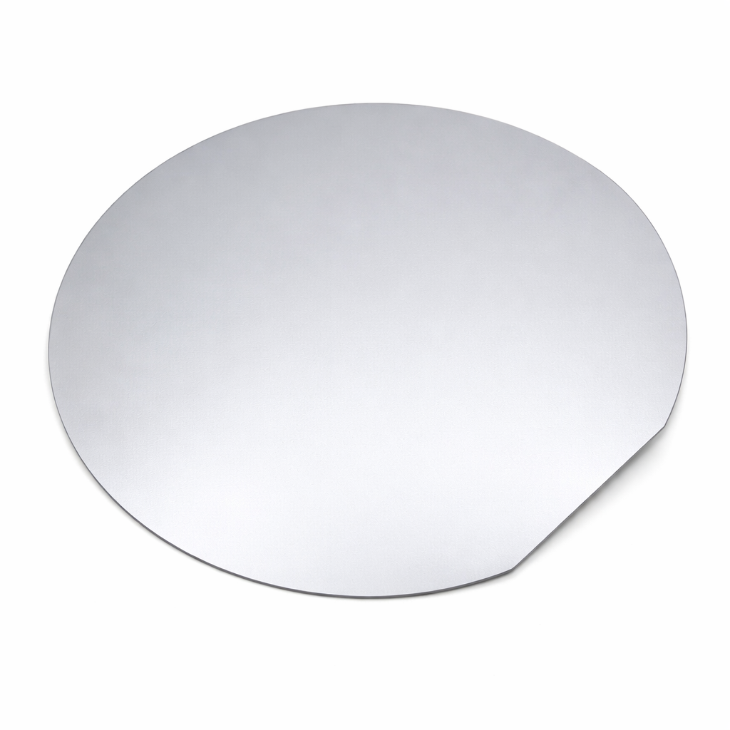
Zinc Oxide (ZnO) Thin Film on Si (100) Wafers
Price range: £178.99 through £262.99
Flat rate shipping £15
Zinc Oxide (ZnO) Thin Film on Si (100) Wafers
Overview
Our zinc oxide (ZnO) thin film wafers are fabricated on high-quality Si (100) substrates to provide uniform, high-quality semiconducting and functional oxide layers for research and device development.
ZnO is a wide bandgap semiconductor with excellent optical transparency, good electrical properties, and piezoelectric characteristics. These wafers are widely used in optoelectronics, sensor development, surface engineering, and thin film device research.
Layer Structure
ZnO (Zinc Oxide layer)
Si (100) substrate
Recommended Film Thickness
50 nm – Surface and interface studies
100 nm – Most popular thickness
200 nm – General optoelectronic applications
Substrate Specifications
Crystal Orientation: Si (100)
Type: N-type
Resistivity: 1–10 Ω·cm
Wafer Thickness: 500–525 µm
Surface Finish: Single-side polished (SSP)
Configuration
Single-side polished + Single-side ZnO (standard)
Double-side coating available upon request.
Film Characteristics
Wide bandgap semiconductor (~3.3 eV)
Good optical transparency
Stable oxide layer
Research-grade thickness uniformity
Applications
UV photodetectors
Optoelectronic device research
Gas sensors
Piezoelectric devices
Surface functionalization
Heterojunction research
Thin film transistor studies
Quality & Packaging
Clean-room compatible handling
Carefully packaged to prevent contamination
Research-grade wafer quality
Custom thickness and wafer sizes available upon request.
| Option 1 | 4″ Si | 100 nm ZnO, 4″ Si | 200 nm ZnO, 4″ Si | 300 nm ZnO, 4″ Si | 50 nm ZnO |
|---|