
LPCVD Si₃N₄ on Si (100) Substrates
Price range: £46.99 through £138.99
Flat rate shipping £15
LPCVD Si₃N₄ on Silicon Substrates (Si (100))
Overview
Our LPCVD silicon nitride (Si₃N₄) substrates are precision-cut from research-grade Si (100) wafers coated with high-density LPCVD silicon nitride films.
LPCVD Si₃N₄ provides excellent film uniformity, high dielectric strength, good mechanical stability, and low defect density, making these substrates suitable for MEMS research, dielectric studies, and microfabrication experiments.
Layer Structure
Si₃N₄ (Silicon Nitride layer)
Si (100) substrate
Recommended Film Thickness
200 nm – Standard dielectric / masking layer
300 nm – Recommended for general microfabrication
500 nm – Thick nitride layer for mechanical structures
Available Sizes
5 × 5 mm
10 × 10 mm
15 × 15 mm
Substrate Specifications
Crystal Orientation: Si (100)
Type: N-type
Resistivity: 1–10 Ω·cm
Surface Finish: Single-side polished (SSP)
Configuration: Single-side Si₃N₄ (standard)
Deposition Process
Low-Pressure Chemical Vapor Deposition (LPCVD)
High film density
Good mechanical stability
Excellent thickness uniformity
Applications
MEMS device prototyping
Hard masking layers
Dielectric isolation research
Mechanical membrane structures
Photonic device platforms
Quality & Packaging
Research-grade wafer quality
Clean-room compatible handling
Carefully packaged to prevent contamination
Custom thickness and sizes available upon request.
| Option 1 | 10 × 10 mm Si | 200 nm LPCVD Si₃N₄, 10 × 10 mm Si | 300 nm LPCVD Si₃N₄, 10 × 10 mm Si | 500 nm LPCVD Si₃N₄, 15 × 15 mm Si | 200 nm LPCVD Si₃N₄, 15 × 15 mm Si | 300 nm LPCVD Si₃N₄, 5 × 5 mm Si | 200 nm LPCVD Si3N4, 5 × 5 mm Si | 300 nm LPCVD Si3N4 |
|---|
Related products
-
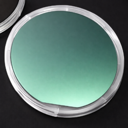
LPCVD Si₃N₄ on Si (100) Wafers
Price range: £226.99 through £382.99