Showing 161–176 of 208 results
-
$1,034.40
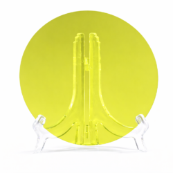
Silicon Carbide (SiC) Single Crystal Substrates (Wafers) Physical Properties (3C-SiC vs 4H-SiC vs 6H-SiC): – Lattice Parameters: – 4H-SiC: a=3.076 Angstrom, c=10.053 Angstrom – 6H-SiC: a=3.073 Angstrom, c=15.117 Angstrom – 3C-SiC: a=4.3596 Angstrom (cubic, zinc blende) – Stacking Sequence: 3C (ABC) / 4H (ABCB) / 6H (ABCACB) – Mohs Hardness: ≈ 9.2 – Density: 3.21…
-
$48.71 – $382.85Price range: $48.71 through $382.85
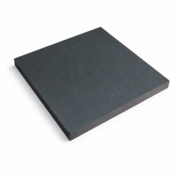
Silicon Carbide (SiC) Ceramic Plates / SiC Structural Ceramic Components Product Overview Silicon Carbide (SiC) ceramic plates are structural ceramics used in extreme temperature and harsh operating environments. Manufactured using pressureless sintering technology, these SiC ceramics have thermal conductivity, oxidation resistance, thermal-shock resistance, and mechanical strength. They are used in high-temperature furnaces, heat treatment systems,…
-
Price upon request
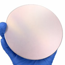
Silicon on Sapphire (SOS) Wafer Substrate Specifications (Sapphire / Al₂O₃): – Material: Al₂O₃ Single Crystal – Orientation: R-plane (1-102) – Diameter: 100 mm (Custom cutting to 5x5mm, 10x10mm available) – Thickness: 460 μm – Flat: One flat Epitaxial Layer Specifications (Silicon Film): – Material: Single Crystal Silicon – Orientation: (100) – Type/Dopant: Undoped – Thickness:…
-
$65.42
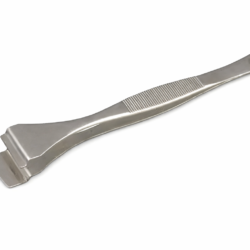
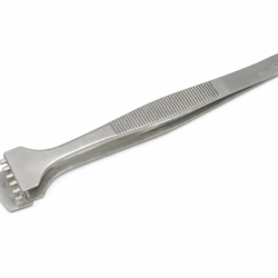
General Specifications (Applicable to All Models) Material: Stainless Steel 302 Magnetism: Non-magnetic Hardness: HRC35 ________________________________________ Model Specifications Model: 91-4T Overall Length: 125 mm Description: Flat wide tip, tip width 12 mm, upper jaw serrated, gap width 1.55 mm ________________________________________ Model: 91-4L Overall Length: 125 mm Description: Flat wide tip, tip width 12 mm, step height…
-
$54.28 – $182.37Price range: $54.28 through $182.37
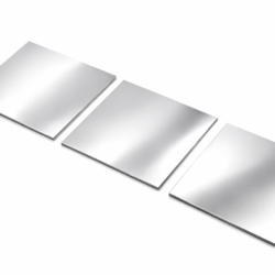
Silver-Coated Silicon Substrates (Ag/Cr on Si (100)) Overview Our silver-coated silicon chips are precision-cut from research-grade Ag thin film wafers fabricated on Si (100) substrates using high-vacuum magnetron sputtering. The controlled deposition process ensures high film uniformity, high reflectivity, and smooth surface morphology. A 5 nm chromium (Cr) adhesion layer is deposited between the silicon…
-
$265.90 – $984.28Price range: $265.90 through $984.28
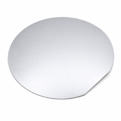
Silver-Coated Silicon Wafers (Ag/Cr on Si (100)) Overview Our silver-coated silicon wafers are fabricated using high-vacuum magnetron sputtering to ensure high film uniformity, high reflectivity, and clean surface morphology. A thin chromium (Cr) adhesion layer (5 nm) is deposited between the silicon wafer and the silver film to has strong interfacial bonding while maintaining standard…
-
$32.01
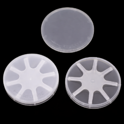
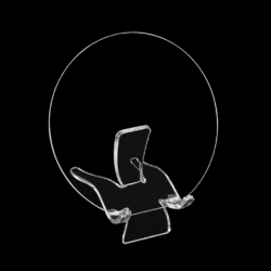
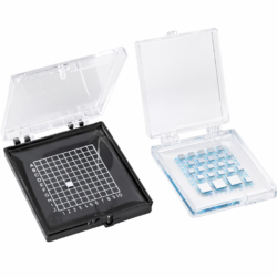
This single-wafer crystal storage box is designed for easy cleaning and convenient assembly. The internal elastic holding structure securely fixes the wafer in place, effectively enhancing safety during transportation and storage. Each crystal box consists of a base, a lid, and an internal elastic fixing insert, providing stable mechanical support and protection for the stored…
-
$666.86
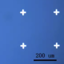
SiO₂ Alignment Cross Mark Wafer (Au Pattern on Si (100)) These alignment-mark silicon wafers feature photolithographically patterned gold cross markers fabricated on thermal silicon dioxide. The cross patterns provide spatial references for microscopy, microfabrication alignment, and microelectrode positioning. The patterned surface supports distance measurement and positioning in micro-scale experiments, and it is used for lithography…
-
$666.86 – $833.92Price range: $666.86 through $833.92
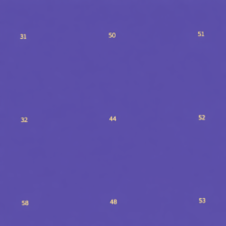
SiO₂ Alignment Mark Wafer (Cr Number Pattern on Si (100)) These thermal silicon dioxide wafers feature photolithographic chromium number patterns designed for alignment, localization, and microfabrication applications. The patterned surface provides indexed micro-scale positioning for electrochemical mapping, MEMS device development, lithography training, and microelectrode alignment. Wafer Specifications Diameter: 4 inch Orientation: Si (100) Resistivity: <…
-
$23.65 – $37.58Price range: $23.65 through $37.58
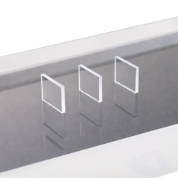
SiO₂ Single Crystal Substrate Physical Properties: – Crystal Structure: Hexagonal System – Lattice Parameters: a=4.914 Angstrom, c=5.405 Angstrom – Density: 2.65 g/cm³ – Melting Point: 1700 °C (Phase transition temp 573.1°C) – Hardness: 7 (Mohs) – Growth Method: Hydrothermal Standard Specifications: 1. Orientation / Cut – Z-cut (001), X-cut (110), Y-cut (100): miscut < 0.3°…
-
$79.34 – $278.43Price range: $79.34 through $278.43
SiO₂ Single Crystal Wafer Physical Properties: – Crystal Structure: Hexagonal System – Lattice Parameters: a=4.914 Angstrom, c=5.405 Angstrom – Density: 2.65 g/cm³ – Melting Point: 1700 °C (Phase transition temp 573.1°C) – Hardness: 7 (Mohs) – Growth Method: Hydrothermal Standard Specifications: 1. Orientation / Cut – Z-cut (001), X-cut (110), Y-cut (100): miscut < 0.3°…
-
$48.71
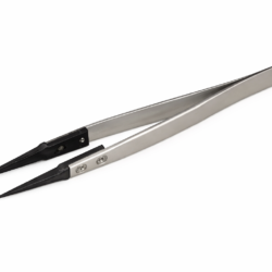
Replaceable Tip Anti-static Stainless Steel Tweezers (ESD Series) Detailed Model Specifications: * ESD-259: Length 120mm | Tip: 0.8mm Point (25mm Long) Application: Applicable for precision electronics repair, laboratory work, semiconductor handling, and jewelry making. The tool has anti-static tips intended to limit electrostatic discharge (ESD) and a stainless steel handle. Features: * ESD Protection: Tips…
-
$19.48
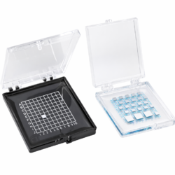
Smarpak SP Series Self-Adsorbing Gel Box, Model 5510 Application: Designed for the storage, transport, and display of optoelectronic components, chips, and samples. The box features a self-adsorbing gel layer that holds devices in place without the need for additional foam or fillers. Features: * Gel Adhesion: The polymer gel layer adsorbs components to hold them…
-
$23.65
Smarpak SP Series Self-Adsorbing Gel Box, Model 7515 Key Specifications: Application: Used for storage, display, and collection of packaged components and small wafers. Feature: Gum surface holds components during transfer/logistics. Avoids use of cotton, foam, or other padding materials. Handling: Allows manual use of tweezers, vacuum pens, or automated equipment for pick-and-place. Cleanliness: gum surface…
-
$165.66 – $243.62Price range: $165.66 through $243.62
Sodium Chloride (NaCl) Single Crystal Window / Substrate Product Overview Sodium Chloride (NaCl) single crystal is an infrared optical material used with high transparency in the mid-infrared region. It is used for IR windows, optical substrates, and spectroscopic applications. NaCl transmission ranges are listed below. Transmission Range: 0.2–25 µm Wavenumber Range: 50000–400 cm⁻¹ Typical Transmission…
-
$162.88 – $165.66Price range: $162.88 through $165.66
Sodium Chloride (NaCl) Single Crystal Substrate Product Overview: NaCl is a water-soluble crystal material and is extremely easy to deliquesce. Please note that because Chemical Mechanical Polishing (CMP) cannot be performed on this material, microscopic scratches may exist on the polished surface. Physical Properties: – Crystal Structure: Cubic System – Lattice Constant: a = 5.6402…