
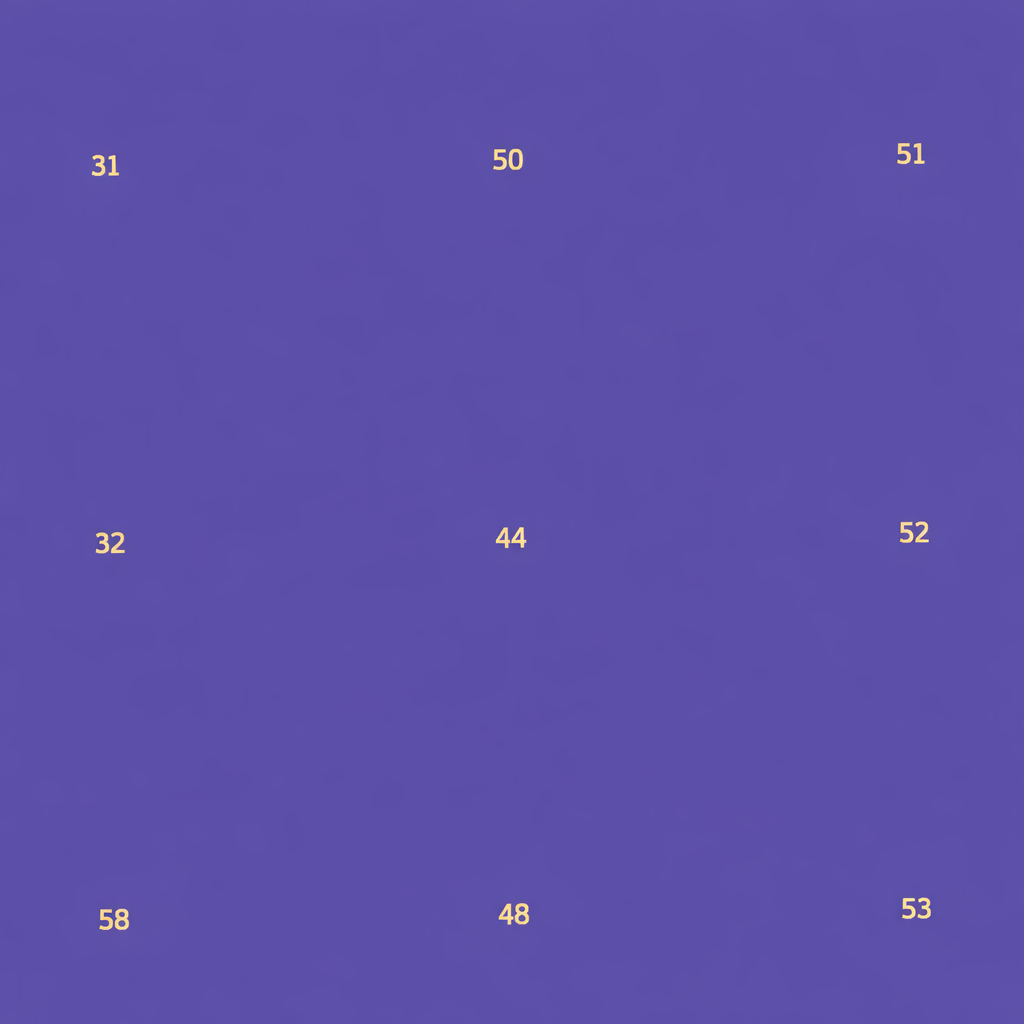
SiO₂ Alignment Mark Wafer (Cr Number Pattern on Si (100))
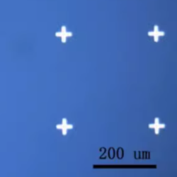
These thermal silicon dioxide wafers feature photolithographic chromium number patterns designed for alignment, localization, and microfabrication applications.
The patterned surface provides indexed micro-scale positioning for electrochemical mapping, MEMS device development, lithography training, and microelectrode alignment.
Wafer Specifications
Diameter: 4 inch
Orientation: Si (100)
Resistivity: < 0.1 Ω·cm
Type: N-type or P-type
Surface: Single-side polished, double-side oxide
Oxide thickness options:
100 nm
300 nm
500 nm
Pattern Specifications
Base grid: 10 × 10 mm per unit
100 numeric markers per unit
Marker spacing: 900 µm
Digit size: 50 µm × 50 µm
Line width: 10 µm
Metal layer: 30 nm Chromium
Fabrication process:
Photolithography → Metal evaporation → Lift-off → Cleaning → Inspection
Applications
– Electrochemical mapping
– Microelectrode positioning
– MEMS device alignment
– Lithography training
– Microfabrication calibration
– Optical microscope reference
Packaging
Individually packed 4-inch wafer
Cleanroom packaging
Custom patterns available upon request.
| Option 1 | 4″ SiO2 (100 nm) | Cr Alignment Pattern | N-Type, 4″ SiO2 (100 nm) | Cr Alignment Pattern | P-Type, 4″ SiO2 (300 nm) | Cr Alignment Pattern | N-Type, 4″ SiO2 (300 nm) | Cr Alignment Pattern | P-Type, 4″ SiO2 (500 nm) | Cr Alignment Pattern | N-Type, 4″ SiO2 (500 nm) | Cr Alignment Pattern | P-Type |
|---|
Related products
-
Thermal SiO₂ on N-Type (Phosphorus-Doped) Si (100) Wafers
Price range: $82.13 through $366.14 -
Thermal SiO₂ on P-type (B-Doped) Si (100) Wafers
Price range: $82.13 through $366.14 -
Thermal SiO₂ on N-Type (As-Doped) Si (100) Wafers
Price range: $82.13 through $366.14 -
-
Thermal SiO₂ on undoped Si (100) Wafers
Price range: $82.13 through $349.43