
Hexagonal Boron Nitride (h-BN) Transferred onto Quartz Substrate (1 cm x 1 cm)
CAS Number: 10043-11-5
Preparation Method:
Hexagonal boron nitride (h-BN) films are initially grown on copper foils using a high-temperature Chemical Vapor Deposition (CVD) process. These quality h-BN films are then transferred onto quartz substrates using a PMMA-assisted wet chemical transfer technique to with uniformity and minimal defects. Morphology Options:
Monolayer
Few Layers (<10 layers, ~5 nm) Multilayer (>5 nm)
All options are available at the same price. For specific requirements, please contact us directly.
Substrate Options:
H-BN films are transferred onto high-purity quartz substrates, with an high combination of transparency, thermal behavior, and chemical inertness. Custom transfer to other substrate materials is available upon request-please visit our Custom Products page or contact us for assistance.
Fundamental Properties:
Hexagonal boron nitride (h-BN) is a two-dimensional material has its standard behavior, insulating properties, and wide bandgap. When transferred onto quartz substrates, it retains its high dielectric and thermal properties, applicable for specialized material applications. Key properties include:
Chemical behavior: High resistance to oxidation and chemical degradation.
Thermal behavior: Applicable to high-temperature environments.
Wide Bandgap: High dielectric properties (bandgap ~5.9 eV), applicable for insulation applications.
Optical Transparency: Combined with quartz, the material with high optical transmission for UV and visible light.
Applications:
Electronics: Applicable as a dielectric layer or insulating substrate for graphene and other 2D materials.
Optoelectronics: Applicable for UV detectors, transparent electronics, and light-emitting devices.
Sensors: A consistent insulating material for gas, chemical, and biosensors.
Thermal Management: Standard thermal insulation and heat dissipation applications. Energy Applications: Relevant as a protective or insulating layer in energy storage and conversion devices.
| Option 1 | Few Layers (<10 layers, ~5 nm), Monolayer, Multilayer (>5 nm) |
|---|
Related products
-

-
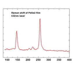
Palladium Diselenide (PdSe₂)
$598.64 -
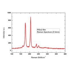
Platinum Diselenide (PtSe₂)
$598.64 -
-
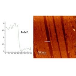
Rhenium Diselenide (ReSe₂)
$598.64 -

Molybdenum Diselenide (MoSe₂)
$598.64 -
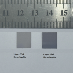
Platinum Ditelluride (PtTe₂)
$598.64 -
Bismuth Telluride (Bi₂Te₃)
$598.64 -
-
Tin Disulfide (SnS₂)
$598.64