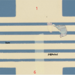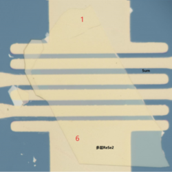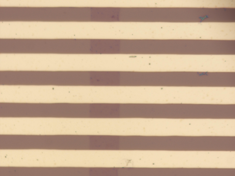
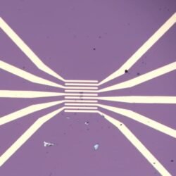
Graphene FET Device
Device Structure:
Conductive Si Substrate / 300 nm SiO₂ Layer / Graphene Channel / Cr+Au Electrodes
Device Description & Features:
Graphene 2D Material: Graphene is a single-layer honeycomb lattice of carbon atoms, offering ultrahigh carrier mobility, linear band dispersion, and tunable electronic properties. Back-Gated FET Configuration: The SiO₂/Si back-gate structure is used for electrostatic-control studies.
Metal Contact Engineering: Cr+Au electrodes for carrier-injection and transport studies. Solution-Processed or CVD-Grown Graphene:
CVD-Grown Monolayer Graphene: For device-fabrication research.
Mechanically Exfoliated Graphene: Preserves intrinsic electronic properties supporting carrier transport.
Applications:
Field-Effect Transistors (FETs):
Graphene FETs exhibit ballistic transport, high-speed switching, and low noise, enabling nanoelectronics. Flexible and Transparent Electronics:
For wearable devices, transparent touchscreens, and flexible transistors due to graphene’s mechanical flexibility and optical transparency. Optoelectronic & Photodetector Devices:
Graphene’s broadband absorption and high carrier mobility can support use in ultrafast photodetectors and THz applications. Quantum Transport & Spintronics:
Graphene’s Dirac-like band structure and long spin coherence length can support use in quantum computing and spintronic applications.
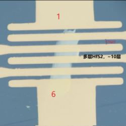
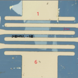
| Option 1 | Few-layer (~5 layers), Multilayer (~10 layers) |
|---|
Related products
-
WSe₂ FET Device
$835.32 -
-
WS₂ FET Device
$835.32 -

-
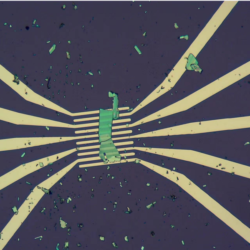
Multilayer ReS₂/PdSe₂ FET Device
$835.32 -
-
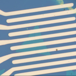
MoS₂ FET Device
$835.32 -
-

Monolayer 2H-MoTe₂ FET Device
$835.32 -