
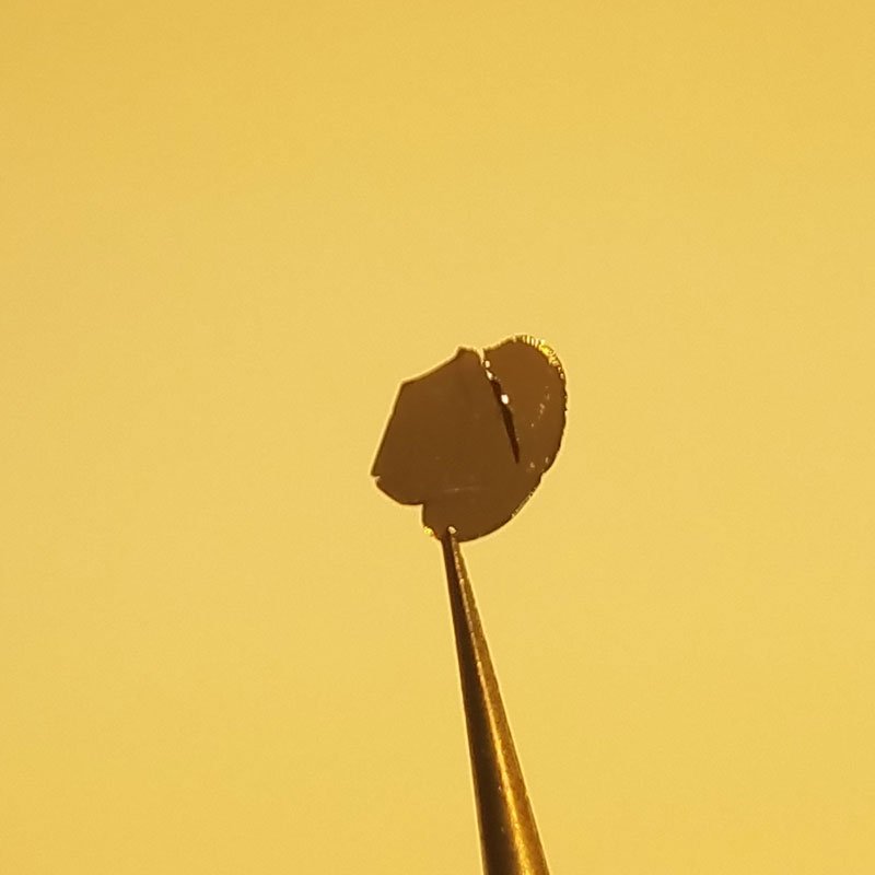
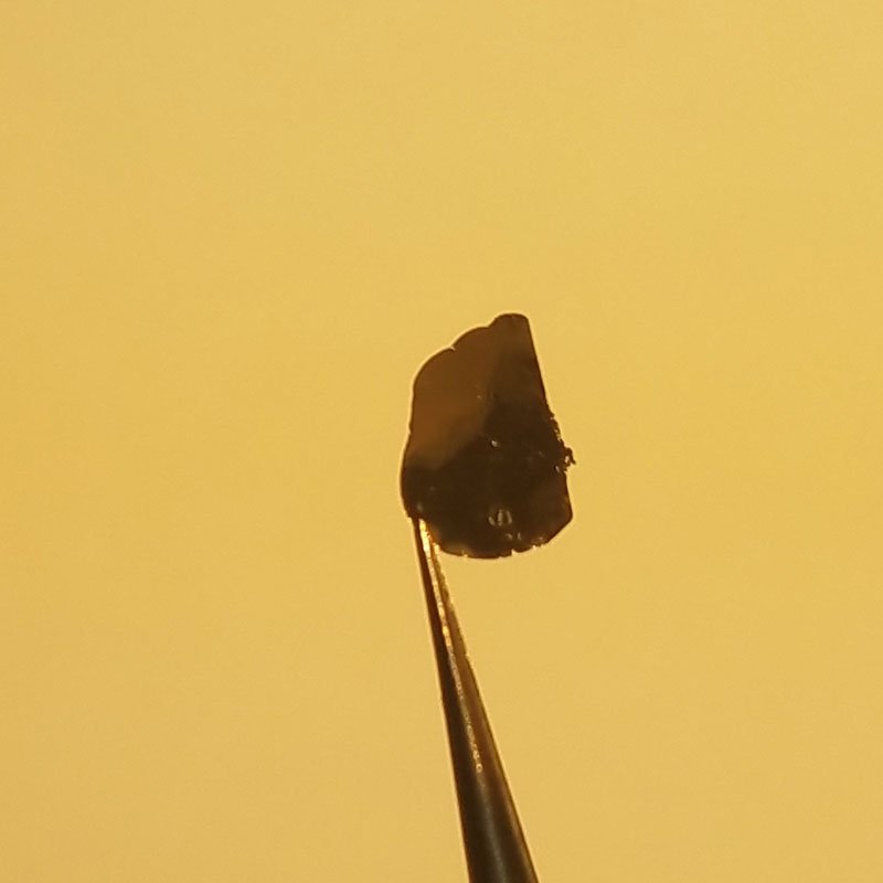
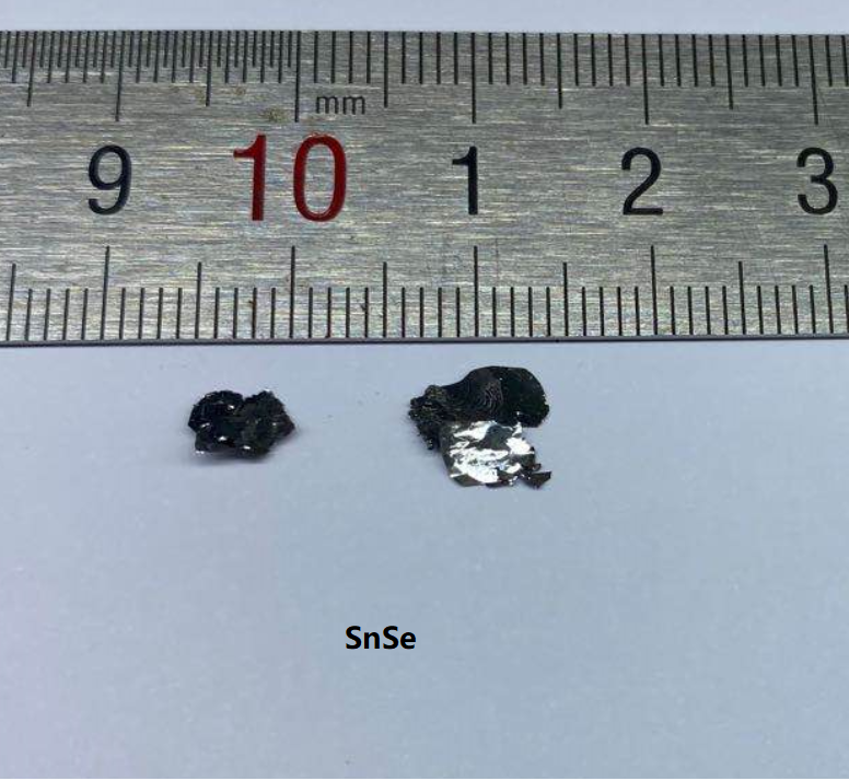
SnSe Crystals
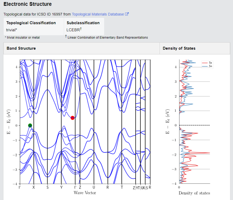
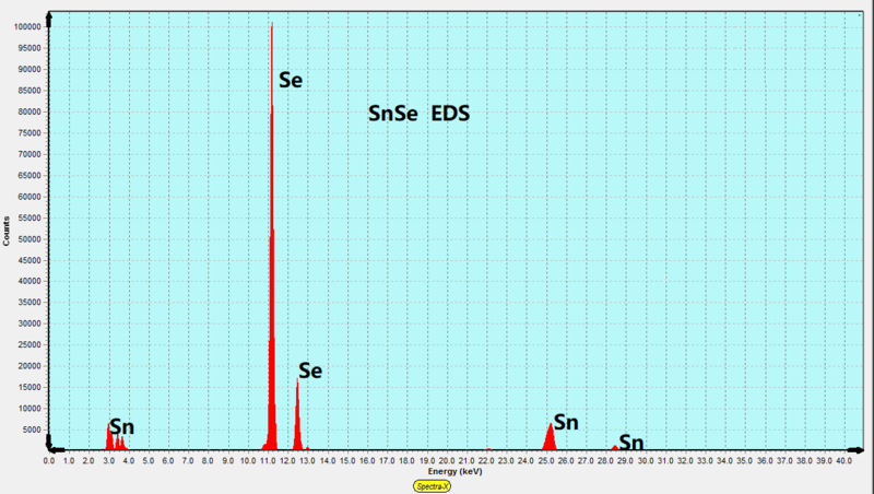
SnSe (Tin Selenide) is a layered semiconductor with an orthorhombic crystal structure and thermoelectric properties characterized by its Seebeck coefficient and low thermal conductivity. It exhibits anisotropic electronic and optical characteristics, supporting applications in thermoelectrics, optoelectronics, nanoelectronics, and 2D material research. SnSe crystals are synthesized using the Chemical Vapor Transport (CVT) method.
Sample Size Options:
Crystals larger than 10 mm²
Crystals larger than 25 mm²
Crystals larger than 100 mm²
Material Properties:
Layered Structure: Facilitates exfoliation into monolayers or few-layer nanosheets for 2D materials research.
Thermoelectric Efficiency: Exhibits a thermoelectric figure of merit (ZT), supporting energy conversion devices.
Anisotropic Electrical Conductivity: Directional dependence of electrical and thermal transport properties.
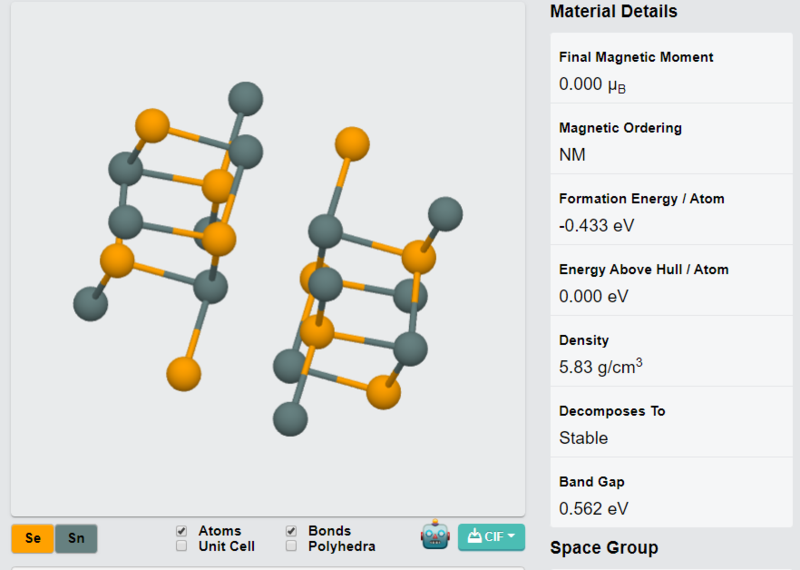
Variable Bandgap: Indirect bandgap of ~0.9 eV in bulk, which can be modified in thin layers, applicable to optoelectronic devices.
Crystal Structure:
Type: Orthorhombic layered structure (Pnma space group)
Features: Layers applicable for thin-film fabrication and device applications.
Degree of Exfoliation:
Ease of Use: Exfoliated into monolayers or few-layer nanosheets for materials research and heterostructure assembly.
Other Characteristics:
Thermoelectric Performance: ZT values for heat-to-electricity conversion.
Optoelectronic Properties: Light absorption and photoconductivity, applicable for infrared detectors and solar cells.
Mechanical Flexibility: Applicable to flexible electronic and thermoelectric devices.
Applications:
Thermoelectric Devices:
Applicable for energy harvesting, cooling applications, and waste heat recovery due to its thermoelectric performance. Optoelectronics:
Applicable to photodetectors, solar cells, and infrared sensing devices. Nanoelectronics:
Used for transistors, logic circuits, and flexible electronic devices.
2D Material Studies:
Applicable for exfoliation into monolayers and assembly into van der Waals heterostructures. Sensors:
Used for gas detection, chemical sensing, and environmental monitoring applications. Synthesis Method:
Chemical Vapor Transport (CVT).
| Option 1 | > 10 mm², > 100 mm², > 25 mm² |
|---|
Related products
-
FeCl₃ Crystals
Price range: $696.09 through $1,252.98 -
Bi Crystals
$696.09 -
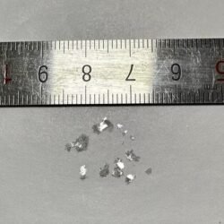
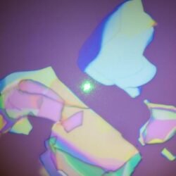
BiOCl Crystals
Price range: $696.09 through $793.55 -
VS₂ Crystals
Price range: $696.09 through $793.55 -
TiS₃ Crystals
Price range: $654.33 through $1,252.98 -
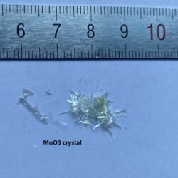
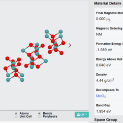
α-MoO₃ Crystals
Price range: $640.41 through $696.09 -
Co₃Sn₂S₂ Crystals
$835.32 -
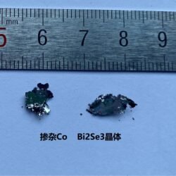
Co-Doped Bi₂Se₃ Crystals
$696.09 -
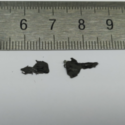
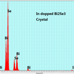
InBiSe₃ Crystals
Price range: $696.09 through $1,252.98 -
WSSe Crystals
Price range: $835.32 through $1,252.98