
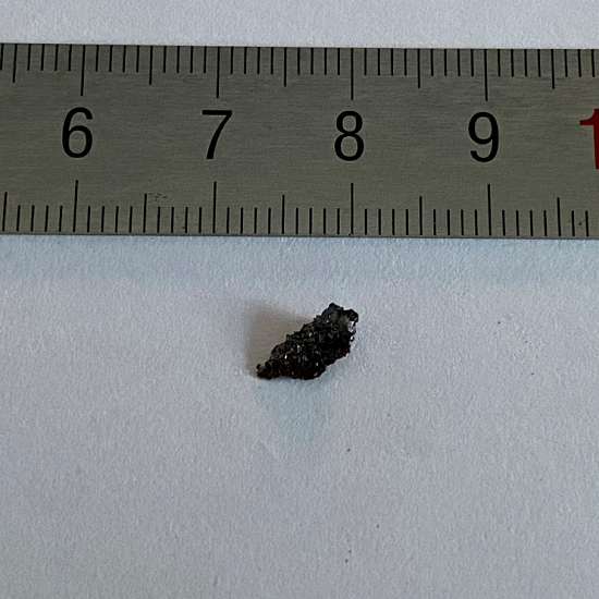
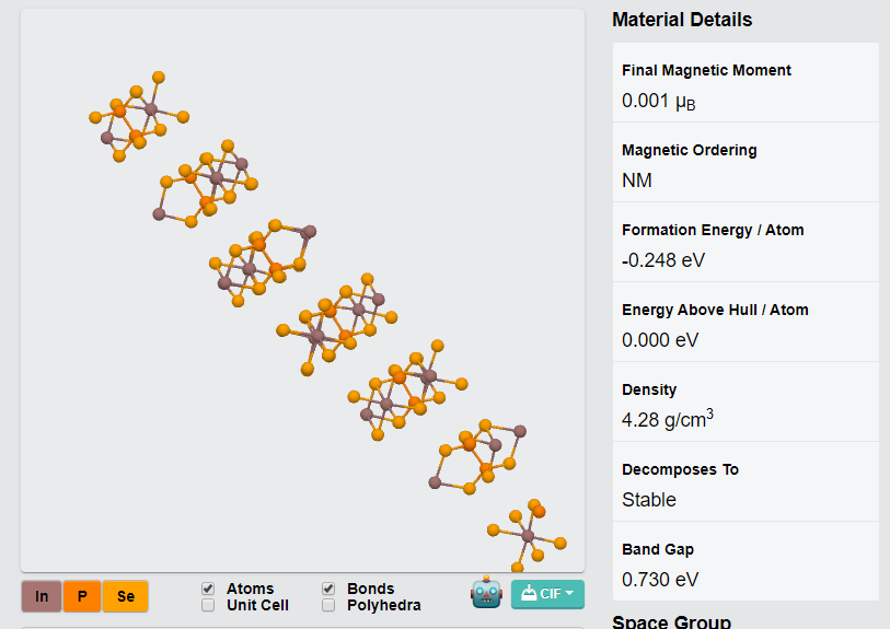
In₂P₃Se₉ Crystals
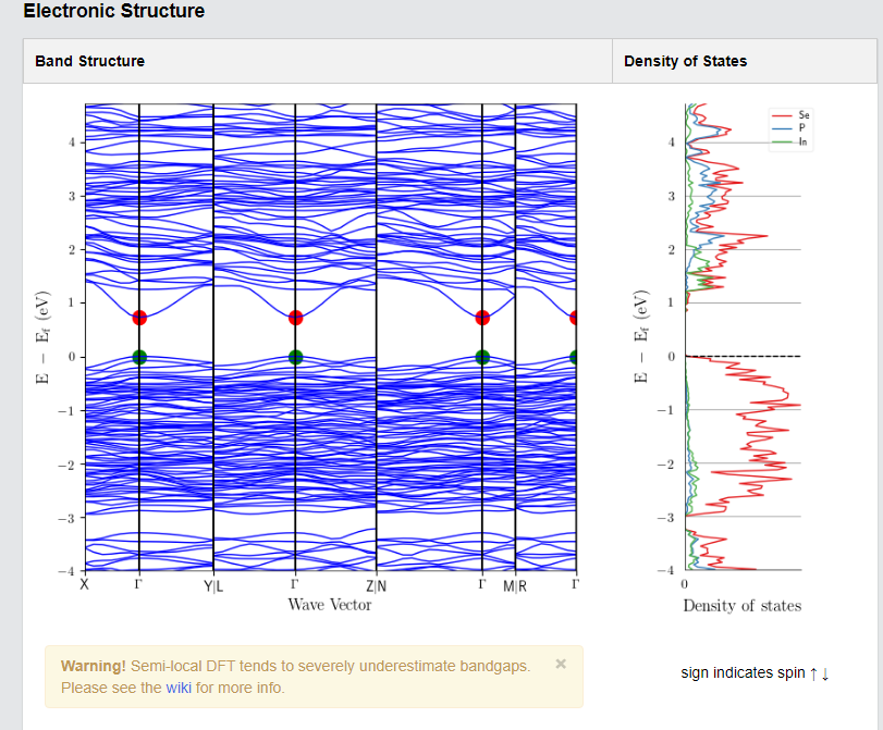
In₂P₃Se₉ is a layered ternary chalcogenide material with a van der Waals structure. It exhibits semiconducting behavior, strong optical absorption, and high environmental behavior, making it an high candidate for optoelectronics, energy storage, and 2D material studies.
Sample Size Options:
Crystals larger than 10 mm²
Crystals larger than 25 mm²
Material Properties:
Layered van der Waals Structure: Facilitates exfoliation into monolayers or few-layer sheets for specialized research.
Semiconducting Behavior: Moderate bandgap applicable to photonic and electronic devices.
Strong Optical Absorption: High absorption in the visible-to-infrared range.
High Environmental behavior: Retains properties under ambient conditions.
Crystal Structure:
Type: Trigonal layered structure
Features: Cleavable layers applicable to thin-film fabrication and nanoscale device assembly.
Degree of Exfoliation:
Ease of Use: Readily exfoliates into thin layers for specialized material studies and applications.
Other Characteristics:
Optoelectronic Performance: High photoconductivity and variable bandgap for specialized devices. Energy
Applications: Applicable to thermoelectric systems and catalytic processes.
Quantum Research Potential: Permits exploration of electronic transport and quantum effects in layered chalcogenides.
Applications:
Optoelectronics:
Applicable for photodetectors, LEDs, and photovoltaic cells. Energy
Applications:
Promising for thermoelectric devices and energy conversion systems. Quantum Materials Research:
Applicable to studying transport phenomena and electronic properties in 2D systems.
2D Material Studies:
Applicable for exfoliation into monolayers and assembly into van der Waals heterostructures. Sensors:
High sensitivity for detecting environmental and chemical stimuli.
| Option 1 | > 10 mm², > 25 mm² |
|---|
Related products
-
WSSe Crystals
Price range: $835.32 through $1,252.98 -
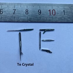
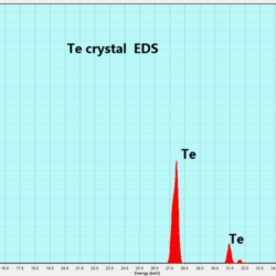
Te Crystals
$696.09 -
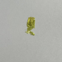
GaS Crystals
Price range: $696.09 through $793.55 -
FeBr₃ Crystals
Price range: $654.33 through $696.09 -
HOPG
$668.25 -
CrBr₃ Crystals
$696.09 -
Ni₂Bi₂Te₅ Crystals
Price range: $696.09 through $793.55 -
GeS Crystals
Price range: $696.09 through $765.70 -
Bi Crystals
$696.09 -
Co-Doped Bi₂Se₃ Crystals
$696.09