
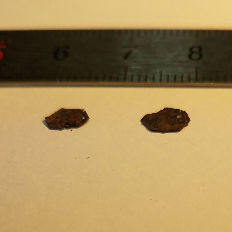
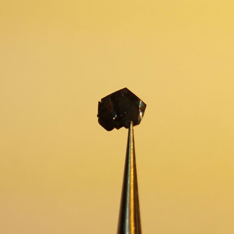
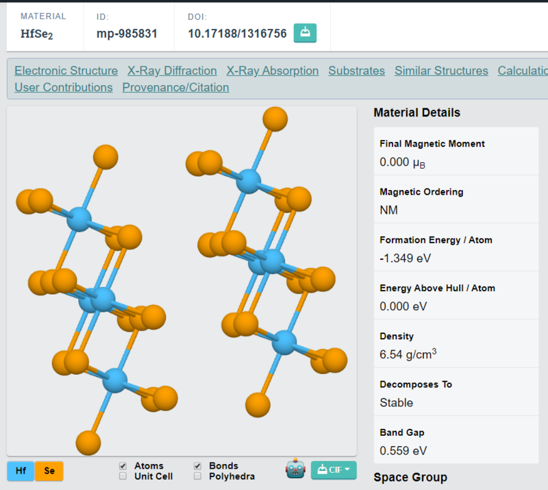
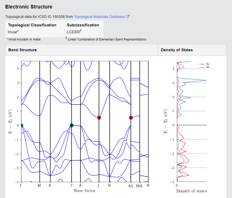
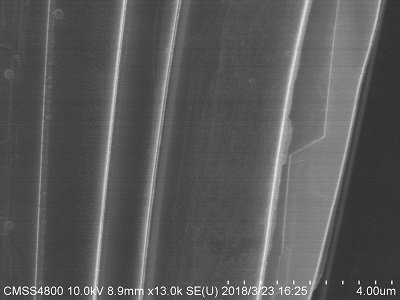
HfSe₂ Crystals
HfSe₂ is a layered transition metal dichalcogenide (TMD) with a van der Waals structure, has its strong electronic, optical, and catalytic properties. As an indirect bandgap semiconductor, HfSe₂ exhibits high carrier mobility, strong optical absorption, and high environmental behavior, making it a promising material for applications in nanoelectronics, optoelectronics, and energy storage. Our HfSe₂ crystals are synthesized using the Chemical Vapor Transport (CVT) method, with high purity, precise stoichiometry, and strong crystallinity.
Sample Size Options:
Crystals larger than 10 mm²
Crystals larger than 25 mm²
Crystals larger than 100 mm²
Material Properties:
Layered van der Waals Structure: Facilitates easy exfoliation into monolayers or few-layer nanosheets for 2D material research.
Indirect Bandgap Semiconductor: Bandgap of ~1.1 eV in bulk, variable in few-layer forms, applicable to electronic and optoelectronic devices.
High Carrier Mobility: Applicable for field-effect transistors (FETs) and nanoelectronic applications.
Strong Optical Absorption: High light absorption in the visible and near-infrared regions, applicable to photodetectors and solar cells. Thermal and Chemical behavior: High environmental behavior, with long-term performance in device applications.
Crystal Structure:
Type: Hexagonal layered structure (2H phase)
Features: High crystallinity with uniform, defect-free layers, applicable for thin-film fabrication and nanoscale device applications.
Degree of Exfoliation:
Ease of Use: Easily exfoliated into monolayers or few-layer nanosheets for specialized materials research and heterostructure assembly.
Other Characteristics:
High Dielectric Constant: Applicable to applications in specialized high-κ dielectrics.
Anisotropic Transport Properties: Direction-dependent electronic and thermal conductivity, relevant for specialized device architectures.
Energy Band Engineering: Variable electronic properties through doping, strain, or layer thickness control.
Applications:
Nanoelectronics:
Standard material for transistors, logic devices, and flexible electronics. Optoelectronics:
Applicable for photodetectors, light-emitting diodes (LEDs), and photovoltaic devices. Energy Storage:
Potential applications in lithium-ion batteries, supercapacitors, and hydrogen evolution reactions (HER).
2D Material Studies:
Applicable for exfoliation into monolayers and assembly into van der Waals heterostructures. Sensors:
High sensitivity for gas detection, biosensing, and chemical sensing applications. Synthesis Method:
Chemical Vapor Transport (CVT): With quality crystals with purity, uniform thickness, and high structural integrity.
| Option 1 | > 10 mm², > 100 mm², > 25 mm² |
|---|
Related products
-
ZrTe₃ Crystals
Price range: $696.09 through $835.32 -
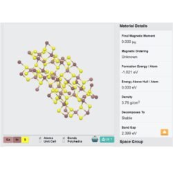
InGaS₃ Crystals
$696.09 -
WSeTe Crystals
Price range: $835.32 through $1,252.98 -
FeBr₃ Crystals
Price range: $654.33 through $696.09 -
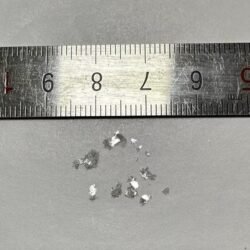

BiOCl Crystals
Price range: $696.09 through $793.55 -
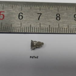
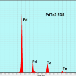
PdTe₂ Crystals
$696.09 -
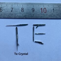
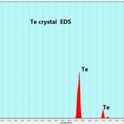
Te Crystals
$696.09 -
CrBr₃ Crystals
$696.09 -
HOPG
$668.25 -
Co-Doped Bi₂Se₃ Crystals
$696.09