Hexagonal Boron Nitride (h-BN) Transferred onto SiO₂ Substrate (1 cm x 1 cm)
CAS Number: 10043-11-5
Preparation Method:
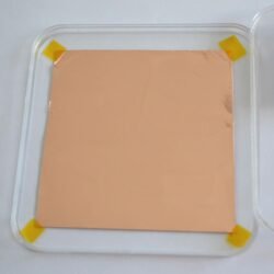
Hexagonal boron nitride (h-BN) films are first grown on copper foils via a high-temperature Chemical Vapor Deposition (CVD) process. These h-BN films are subsequently transferred onto SiO₂/Si substrates (300 nm SiO₂ layer) using a PMMA-assisted wet chemical transfer method to produce films with minimal defects. Morphology Options:
Monolayer
Few Layers (<10 layers, ~5 nm) Multilayer (>5 nm)
All options are available at the same price. For specific requirements, please contact us directly.
Substrate Options:
H-BN films are transferred onto SiO₂/Si substrates, with an insulating base for the listed applications. Custom transfer to other substrate materials is available upon request; please visit Custom Products page or contact us for assistance.
Fundamental Properties:
Hexagonal boron nitride (h-BN) is a two-dimensional material with insulating properties. Transferred h-BN films retain their dielectric and mechanical properties, combined with the thermal behavior of the SiO₂/Si substrate. Listed properties include:
Chemical behavior: Resistance to oxidation and chemical degradation.
Thermal behavior: Can withstand high temperatures.
Mechanical Strength: Strength and flexibility permit assembly into devices.
Wide Bandgap: Dielectric properties (bandgap ~5.9 eV) for use as an insulating layer.
Applications:
Electronics: Applicable as a dielectric layer or insulating substrate for graphene and other 2D materials in electronic devices.
Optoelectronics: Applicable to light-emitting devices and UV detectors.
Thermal Management: Applicable for thermal insulation and heat dissipation.
Sensors: A chemically resistant insulating material for gas and chemical sensors. Energy Applications: Used as a protective or insulating layer in energy storage and conversion devices.
| Option 1 | Few Layers (<10 layers, ~5 nm), Monolayer, Multilayer (>5 nm) |
|---|
Related products
-

-
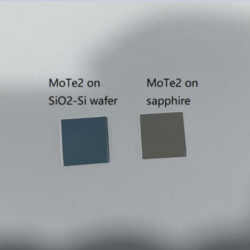
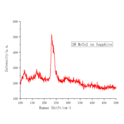
Molybdenum Ditelluride (MoTe₂)
$598.64 -
Bismuth Telluride (Bi₂Te₃)
$598.64 -
-
Tin Diselenide (SnSe₂)
$598.64 -
-
-
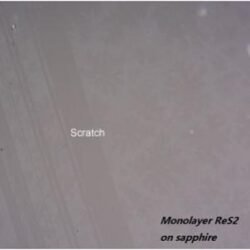
Rhenium Disulfide (ReS₂)
$598.64 -
-