Graphene Transferred onto SiO₂ Substrate (1 cm x 1 cm)
CAS Number: 7782-42-5
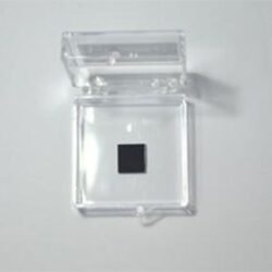
Substrate Size: 1 cm x 1 cm
Preparation Method: Graphene film is grown on copper foils via Chemical Vapor Deposition (CVD) and transferred onto SiO₂/Si substrates with a 300 nm SiO₂ layer using a PMMA (polymethyl methacrylate) layer and wet chemical transfer techniques. Morphology Options:
Continuous Monolayer Film
Continuous Multilayer Film
Applications include specific requirements, please contact us directly.
Substrate Options:
Graphene film is transferred onto SiO₂/Si substrates with a 300 nm SiO₂ layer. Custom transfer to other substrate materials is available upon request-please visit our Custom Products page or contact us for assistance.
Fundamental Properties:
Graphene film transferred onto SiO₂/Si substrates with a 300 nm SiO₂ layer retains its high electronic, optical, and mechanical properties while leveraging the fit and unique properties of the SiO₂/Si substrate. The 300 nm SiO₂ layer has specified optical contrast for graphene visualization under optical microscopes. Key properties include: Electrical Properties: High electrical conductivity with carrier mobility above 10,000 cm²/V-s. Typical sheet resistance <=500 Ω/sq (monolayer) and <=100 Ω/sq (multilayer). Low Raman D/G ratio confirms minimal defect density after PMMA-assisted wet transfer.
Optical Properties: Enhanced optical contrast of graphene on the 300 nm SiO₂ layer facilitates easy identification and characterization using standard optical microscopy.
Mechanical Properties: High strength and flexibility, with a tensile strength of ~130 GPa.
Thermal Properties: High thermal conductivity of graphene combined with the thermal behavior of the SiO₂/Si substrate, applicable for specialized device applications.
Applications: Semiconductor Research: SiO₂/Si substrates are used for graphene-based device prototyping, including transistors, sensors, and other nanoelectronic devices.
Optoelectronics: Graphene on SiO₂/Si substrates can be utilized for photodetectors, transparent conductive films, and other optoelectronic devices.
Sensors: Applicable for gas, chemical, and biological detection, benefiting from graphene’s conductivity and high surface area. Quantum and Nanoelectronics: The combination of graphene and SiO₂/Si is used for exploring quantum effects and fabricating nanoscale devices. Microscopy and Characterization: The 300 nm SiO₂ layer has high optical contrast, permits straightforward visualization and characterization of graphene layers under optical microscopes.
| Option 1 | Continuous Monolayer Film, Continuous Multilayer Film |
|---|
Related products
-
Nickel Ditelluride (NiTe₂)
$598.64 -

-
Molybdenum Diselenide (MoSe₂)
$598.64 -
-
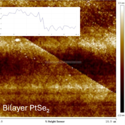
Platinum Diselenide (PtSe₂)
$598.64 -
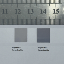
Platinum Ditelluride (PtTe₂)
$598.64 -
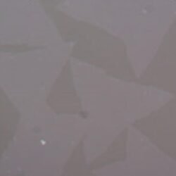
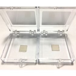
Tungsten Diselenide (WSe₂)
$598.64 -
Antimony Telluride (Sb₂Te₃)
$598.64 -
Bismuth Selenide (Bi₂Se₃)
$598.64 -