
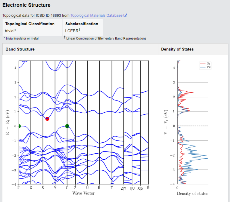
PdSe₂ Crystals
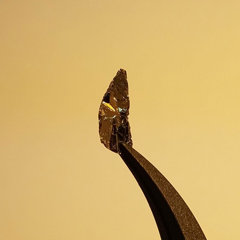
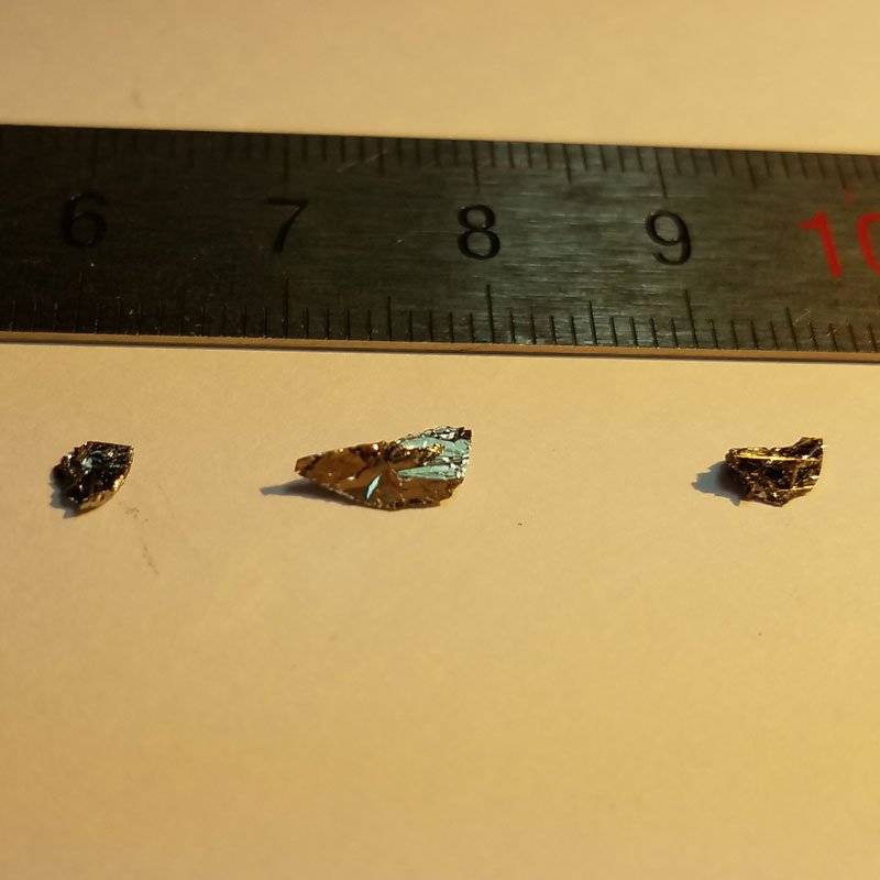
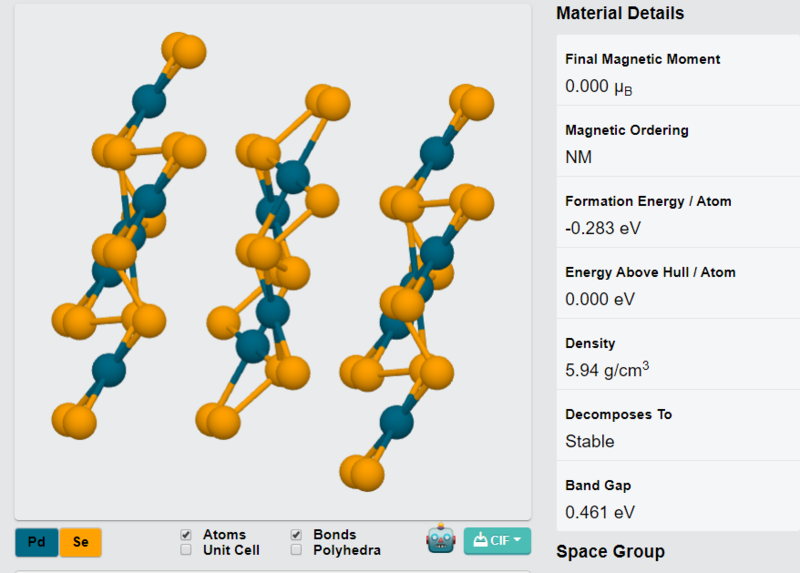
PdSe₂ is a layered transition metal dichalcogenide (TMD) with pentagonal crystal structure and variable electronic properties. Unlike typical TMDs, PdSe₂ exhibits a transition from semimetallic behavior in bulk to semiconducting properties in monolayer form. It also features carrier mobility and anisotropic optical and electrical characteristics, supporting applications in nanoelectronics, optoelectronics, sensing, and energy-related devices. PdSe₂ crystals are synthesized using the Chemical Vapor Transport (CVT) method.
Sample Size Options:
Crystals larger than 10 mm²
Crystals larger than 25 mm²
Material Properties:
Pentagonal Structure: Distinct from traditional hexagonal TMDs, associated with anisotropic properties. Semiconducting-to-Semimetallic Transition: Indirect bandgap of ~1.3 eV in monolayer form, transitioning to semimetallic behavior in bulk.
Carrier Mobility: Applicable to high-speed field-effect transistors (FETs) and nanoelectronic devices.
Anisotropic Properties: Direction-dependent optical and electronic behavior for material research.
Environmental behavior: Resistant to degradation under ambient conditions.
Crystal Structure:
Type: Orthorhombic layered structure with pentagonal lattice symmetry
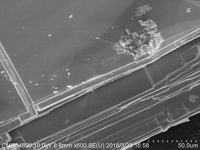
Features: Layers applicable for thin-film fabrication and nanoscale device assembly.
Degree of Exfoliation:
Ease of Use: Exfoliated into monolayers or few-layer nanosheets for materials research and heterostructure assembly.
Other Characteristics:
Optical Absorption: Used in photodetectors and light-harvesting devices.
Anisotropic Transport: Permits exploration of direction-dependent transport phenomena in quantum devices.
Chemical behavior: Maintains structural integrity in air, advantageous for long-term sensing applications.
Applications:
Nanoelectronics:
Used for transistors, logic devices, and flexible electronics. Optoelectronics:
Applicable for photodetectors, light-emitting diodes (LEDs), and photovoltaic devices due to light-matter interactions. Sensors:
Used for gas detection, chemical sensing, and biosensing applications. Energy Storage and Catalysis:
Potential for applications in energy storage devices, hydrogen evolution reactions (HER), and catalysis.
2D Material Studies:
Applicable for exfoliation into monolayers and assembly into van der Waals heterostructures. Synthesis Method:
Chemical Vapor Transport (CVT).
| Option 1 | > 10 mm², > 25 mm² |
|---|
Related products
-
VS₂ Crystals
Price range: $696.09 through $793.55 -
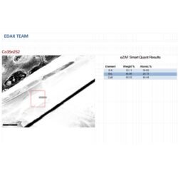
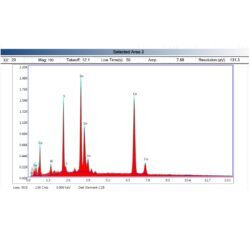
Co₃Sn₂S₂ Crystals
$835.32 -
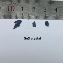
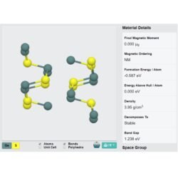
GeS Crystals
Price range: $696.09 through $765.70 -
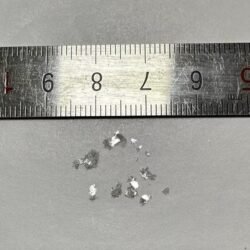

BiOCl Crystals
Price range: $696.09 through $793.55 -
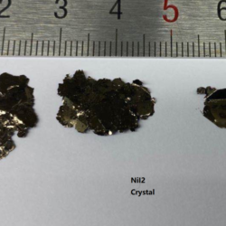
NiI₂ Crystals
Price range: $696.09 through $1,390.81 -
PdTe₂ Crystals
$696.09 -
WSeTe Crystals
Price range: $835.32 through $1,252.98 -
Bi Crystals
$696.09 -
GeSe₂ Crystals
Price range: $696.09 through $793.55 -
ZrTe₃ Crystals
Price range: $696.09 through $835.32