
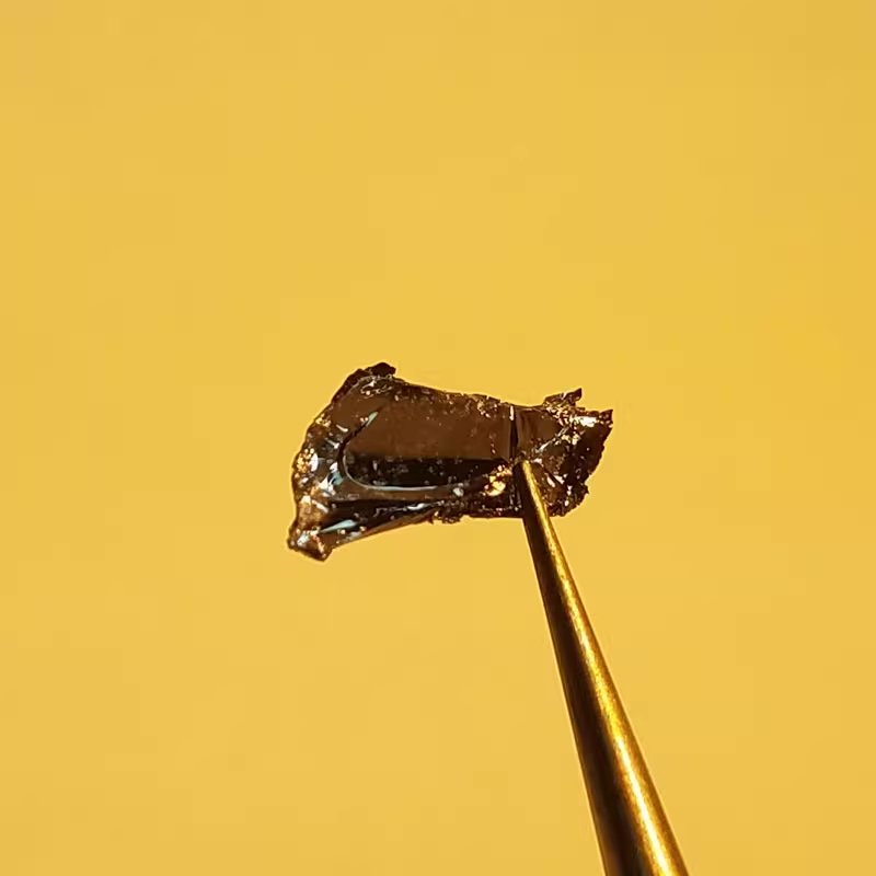
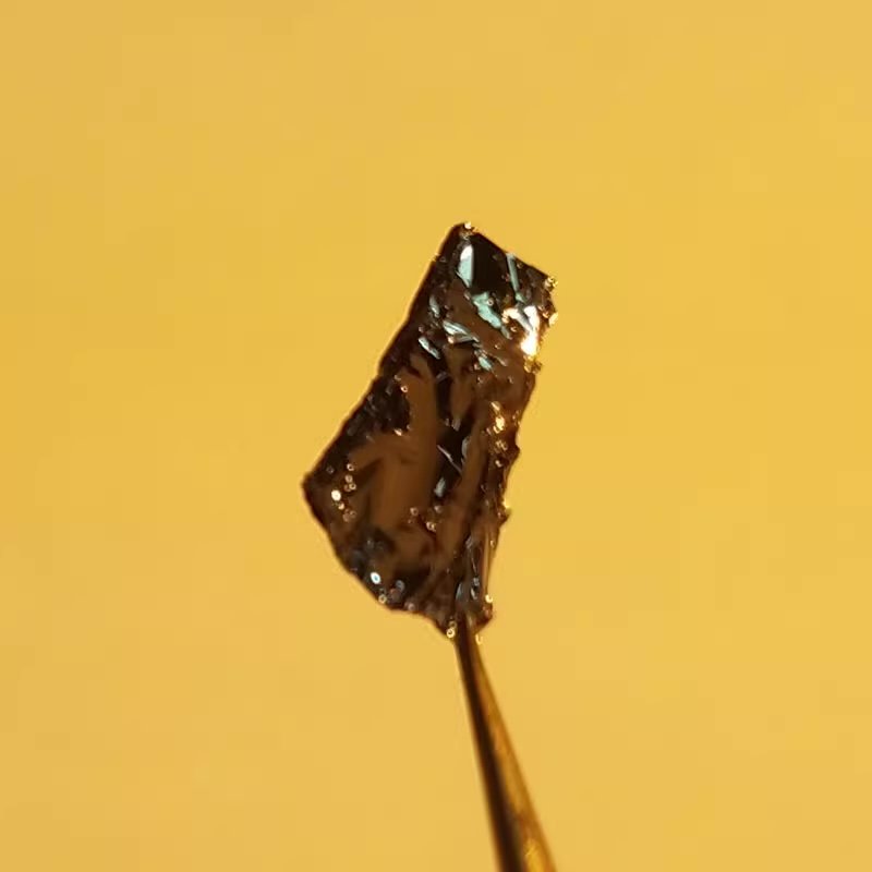
MoSSe Crystals
MoSSe is a Janus-type layered transition metal dichalcogenide (TMD) with asymmetric sulfur and selenium layers, standard to unique physical and chemical properties. Its broken out-of-plane symmetry results in a built-in dipole moment, enhancing piezoelectric, optoelectronic, and catalytic performance. MoSSe is investigated for applications in 2D materials, quantum devices, and energy conversion technologies. Our MoSSe crystals are synthesized using the Chemical Vapor Transport (CVT) method, with high purity, precise stoichiometry, and high crystallinity.
Sample Size Options:
Crystals larger than 10 mm²
Crystals larger than 25 mm²
Crystals larger than 100 mm²
Material Properties:
Janus Structure (Asymmetric Mo-S/Se Layers): Results in a built-in dipole moment, permits strong piezoelectric and ferroelectric effects.
Variable Bandgap: Direct-to-indirect bandgap transition depending on thickness, with bandgaps ranging from ~1.5 eV to ~1.8 eV.
High Carrier Mobility: Applicable to high-speed electronic and optoelectronic devices.
Strong Spin-Orbit Coupling: Facilitates spintronic applications and valleytronics research.
Enhanced Catalytic Activity: High surface reactivity for electrocatalysis, particularly in hydrogen evolution reactions (HER).
Crystal Structure:
Type: Hexagonal layered structure with Janus symmetry
Features: Cleavable layers applicable for thin-film fabrication and nanoscale device applications.
Degree of Exfoliation:
Ease of Use: Easily exfoliated into monolayers or few-layer nanosheets for 2D materials research and device assembly.
Other Characteristics:
Piezoelectric and Ferroelectric Effects: Due to out-of-plane dipole asymmetry, making it applicable to nanoscale sensors and actuators.
High Optical Absorption: Applicable for optoelectronic applications, including photodetectors and solar cells.
Quantum Confinement Effects: Exhibits unique quantum properties when thinned down to monolayer structures.
Applications:
Optoelectronics:
Applicable for photodetectors, light-emitting diodes (LEDs), and solar cells due to strong light-matter interaction. Spintronics & Valleytronics:
Applicable to spin-based devices and valleytronic applications due to strong spin-orbit coupling. Energy Conversion:
High catalytic activity for hydrogen evolution reactions (HER) and other electrocatalytic applications.
2D Material Studies:
Applicable for exfoliation into monolayers and assembly into van der Waals heterostructures. Sensors:
High sensitivity for gas, chemical, and strain sensing due to asymmetric structure and surface activity. Synthesis Method:
Chemical Vapor Transport (CVT): With quality crystals with purity, uniformity, and structural integrity.
| Option 1 | > 10 mm², > 100 mm², > 25 mm² |
|---|
Related products
-
Bi Crystals
$696.09 -
BiOCl Crystals
Price range: $696.09 through $793.55 -
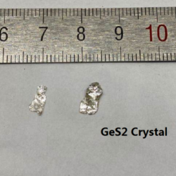
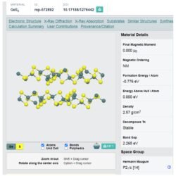
GeS₂ Crystals
Price range: $696.09 through $835.32 -
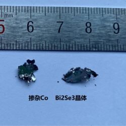
Co-Doped Bi₂Se₃ Crystals
$696.09 -
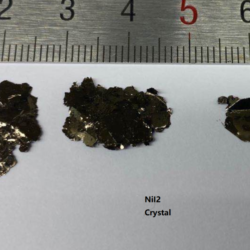
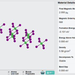
NiI₂ Crystals
Price range: $696.09 through $1,390.81 -
TiS₃ Crystals
Price range: $654.33 through $1,252.98 -
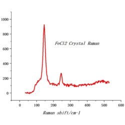
FeCl₂ Crystals
Price range: $696.09 through $793.55 -
NiI₃ Crystals
Price range: $696.09 through $1,252.98 -
VS₂ Crystals
Price range: $696.09 through $793.55 -
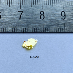
InGaS₃ Crystals
$696.09