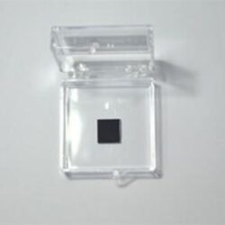
Graphene Transferred onto Sapphire Substrate (1 cm x 1 cm)
CAS Number: 7782-42-5
Substrate Size: 1 cm x 1 cm
Preparation Method: Graphene film is grown on copper foils via Chemical Vapor Deposition (CVD) and transferred onto sapphire substrates using a PMMA (polymethyl methacrylate) layer and wet chemical transfer techniques. Morphology Options:
Continuous Monolayer Film
Continuous Multilayer Film
For specific requirements, please contact us directly.
Substrate Options:
Graphene film is transferred onto sapphire substrates. Custom transfer to other substrate materials is available upon request; please visit Custom Products page or contact us for assistance.
Fundamental Properties:
Graphene transferred onto sapphire substrates retains its electronic, optical, and mechanical properties while benefiting from the characteristics of sapphire, such as thermal behavior, transparency, and electrical insulation. The PMMA-assisted transfer produces graphene films for photonic, optoelectronic, and high-temperature applications. Listed properties include:
Electrical Properties: Electrical conductivity with carrier mobility above 10,000 cm²/V-s. Typical sheet resistance <=500 Ω/sq (monolayer) and <=100 Ω/sq (multilayer). Low Raman D/G ratio confirms minimal defect density after PMMA-assisted wet transfer.
Optical Transparency: Graphene on sapphire transmits ~97.7% of visible light and supports use in transparent and optoelectronic devices.
Mechanical Properties: Strength and flexibility, with a tensile strength of ~130 GPa, supporting the listed applications.
Thermal Properties: Graphene thermal conductivity and sapphire thermal behavior support high-temperature and heat-dissipation applications.
Applications:
Optoelectronics: Applicable for transparent conductive films in displays, photodetectors, and photovoltaic devices, leveraging the sapphire substrate’s optical clarity and thermal behavior.
Sensors: Graphene on sapphire is applicable to gas, chemical, and biological sensing applications due to its conductivity and large surface area. High-Temperature Electronics: The thermal behavior of sapphire substrates makes them applicable to graphene-based devices operating in high-temperature environments.
Photonics: The combination of graphene’s optical properties and sapphire’s transparency supports use in photonic devices and waveguides. Energy Applications: Utilized in transparent electrodes for energy storage devices, such as supercapacitors and batteries, with added behavior from the sapphire substrate.
| Option 1 | Continuous Monolayer Film, Continuous Multilayer Film |
|---|
Related products
-
Tin Disulfide (SnS₂)
$598.64 -

-
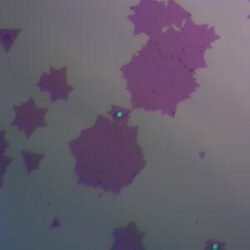
Tin Diselenide (SnSe₂)
$598.64 -
-
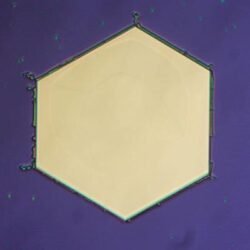
Nickel Ditelluride (NiTe₂)
$598.64 -
Palladium Diselenide (PdSe₂)
$598.64 -
Platinum Diselenide (PtSe₂)
$598.64 -
-
Antimony Telluride (Sb₂Te₃)
$598.64 -