
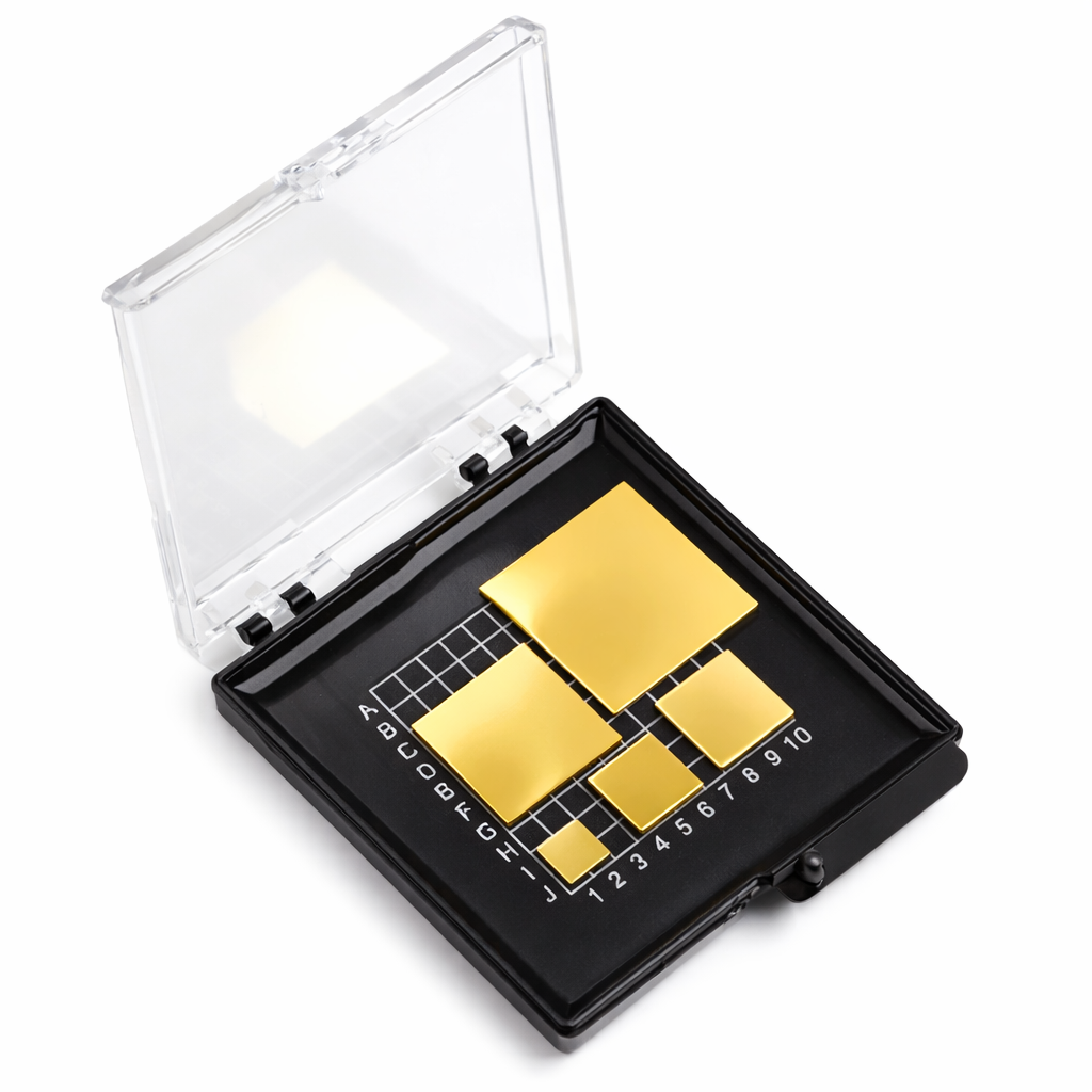
Gold-Coated Silicon Substrates (Au/Ti on Si (100))
Overview
Our gold-coated silicon substrates are fabricated using high-vacuum magnetron sputtering or thermal evaporation to ensure uniform thickness, strong adhesion, and clean surface morphology applicable to research and device fabrication.
A standard 10 nm titanium (Ti) adhesion layer is deposited between the silicon substrate and the gold layer to has high film behavior and long-term reliability.
This product is applicable for electrochemical research, microfabrication, MEMS development, RF structures, and sensor platforms.
Layer Structure
Standard structure:
Au (Gold layer)
Ti (10 nm adhesion layer)
Si (100) substrate
Adhesion Layer
Standard adhesion layer:
Ti (10 nm)
This configuration is used in research laboratories and microfabrication processes due to its high fit with Si/SiO₂ and consistent performance in electrochemical environments.
Custom adhesion thickness available upon request.
Gold Thickness Options
Standard Au thickness:
50 nm
100 nm
500 nm
Custom thickness available upon request.
Substrate Specifications
Standard configuration (default)
Orientation: Si (100)
Doping: N-type, 1–10 Ω·cm resistivity (phosphorus-doped)
Surface finish: Single-side polished (SSP)
This configuration is used in research laboratories, electrochemistry, and microfabrication.
Custom options available upon request
Doping: N-type or P-type
Surface finish: SSP or DSP
Custom resistivity range
Please contact us for special requirements or bulk orders.
Deposition Process
High-vacuum magnetron sputtering
Thermal evaporation (depending on thickness requirement)
Controlled deposition ensures uniform thickness and strong adhesion across the silicon surface.
Applications
Microelectrode fabrication
Electrochemical studies (HER, OER, CO2RR)
MEMS device development
RF and microwave structures
Bonding pads
Sensor and biosensor platforms
Micro-patterned gold devices
Quality & Packaging
Uniform film thickness control
Clean-room fits handling
Protective packaging to prevent contamination
Research-grade surface quality
Why Choose Our Au on Si Substrates?
Research-grade quality
Specified thickness selection
Competitive direct-manufacturer pricing
Custom Orders
We support:
Custom wafer diameter
Custom gold thickness
Patterned gold upon request
Contact us for technical consultation and academic pricing.
| Option 1 | 10 × 10 mm Si | 100 nm Au, 10 × 10 mm Si | 50 nm Au, 10 × 10 mm Si | 500 nm Au, 15 × 15 mm Si | 100 nm Au, 15 × 15 mm Si | 50 nm Au, 20 × 20 mm Si | 100 nm Au, 20 × 20 mm Si | 50 nm Au, 5 × 5 mm Si | 100 nm Au, 5 × 5 mm Si | 50 nm Au, 5 × 5 mm Si | 500 nm Au |
|---|
Related products
-
Gold-Coated Silicon Wafers (Au/Ti or Au/Cr on Si)
Price range: $316.02 through $1,218.17