
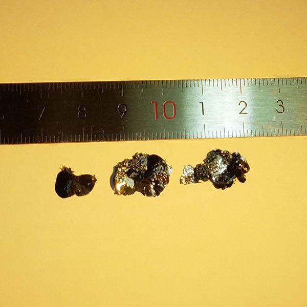

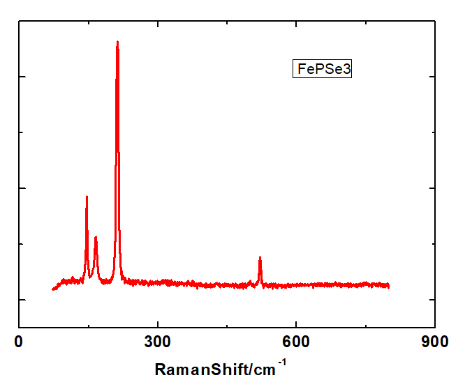
FePSe₃ Crystals
FePSe₃ is a layered antiferromagnetic semiconductor with a van der Waals structure, exhibiting strong in-plane magnetic anisotropy and high electronic properties. It belongs to the MPX3 family (M = transition metal, X = chalcogen), has variable magnetic behavior and semiconducting characteristics. This material is applicable for applications in spintronics, quantum materials research, and 2D magnetism studies. Our FePSe₃ crystals are synthesized using the Chemical Vapor Transport (CVT) method, with high purity, precise stoichiometry, and high crystallinity.
Sample Size Options:
Crystals larger than 10 mm²
Crystals larger than 25 mm²
Crystals larger than 100 mm²
Material Properties:
Layered van der Waals Structure: Facilitates easy exfoliation into monolayers or few-layer sheets for 2D material studies.
Antiferromagnetic Ordering: Exhibits Néel-type antiferromagnetic behavior with strong magnetic anisotropy below ~110 K.
Semiconducting Properties: Moderate bandgap (~1.3-1.5 eV), applicable to optoelectronic and electronic applications.
Magnetic Anisotropy: Strong in-plane magnetic interactions, permits specialized spintronic applications.
Crystal Structure:
Type: Monoclinic layered structure
Features: Cleavable layers, applicable for thin-film fabrication and nanoscale device research.
Degree of Exfoliation:
Ease of Use: Readily exfoliated into thin layers for specialized materials research and device applications.
Other Characteristics:
Quantum Magnetism: Permits exploration of 2D antiferromagnetism, spin-lattice interactions, and quantum spin phenomena.
Spintronic Potential: Promising for spin-based memory devices, magnetic sensors, and data storage technologies.
Environmental behavior: Maintains structural and magnetic properties under ambient conditions.
Applications:
Quantum Materials Research:
Applicable for studying 2D magnetism, quantum spin dynamics, and low-dimensional magnetic systems. Spintronics:
Applicable to magnetic memory devices, spin valves, and spin-based logic circuits.
2D Material Studies:
Applicable for exfoliation into monolayers and assembly into van der Waals heterostructures. Optoelectronics:
Promising for photodetectors, light-emitting devices, and optical modulators. Energy
Applications:
Potential for catalytic applications, energy storage, and specialized battery technologies. Synthesis Method:
Chemical Vapor Transport (CVT): With quality crystals with purity, uniformity, and structural integrity.
| Option 1 | > 10 mm², > 100 mm², > 25 mm² |
|---|
Related products
-
Ni₂Bi₂Te₅ Crystals
Price range: $696.09 through $793.55 -
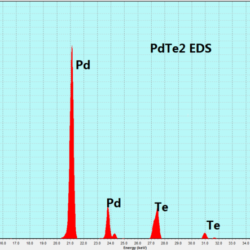
PdTe₂ Crystals
$696.09 -
FeCl₃ Crystals
Price range: $696.09 through $1,252.98 -
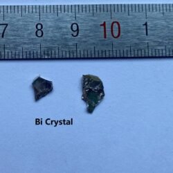
Bi Crystals
$696.09 -
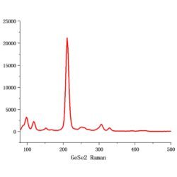
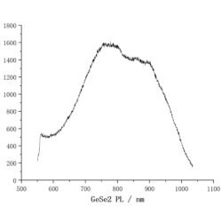
GeSe₂ Crystals
Price range: $696.09 through $793.55 -
FeBr₃ Crystals
Price range: $654.33 through $696.09 -
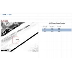
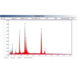
Co₃Sn₂S₂ Crystals
$835.32 -
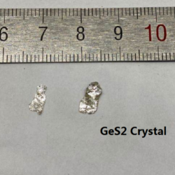
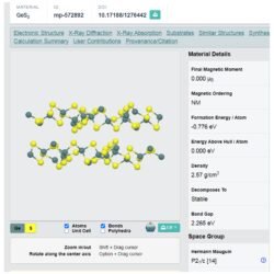
GeS₂ Crystals
Price range: $696.09 through $835.32 -
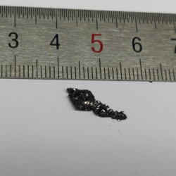
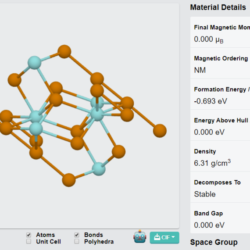
ZrTe₃ Crystals
Price range: $696.09 through $835.32 -
HOPG
$668.25