
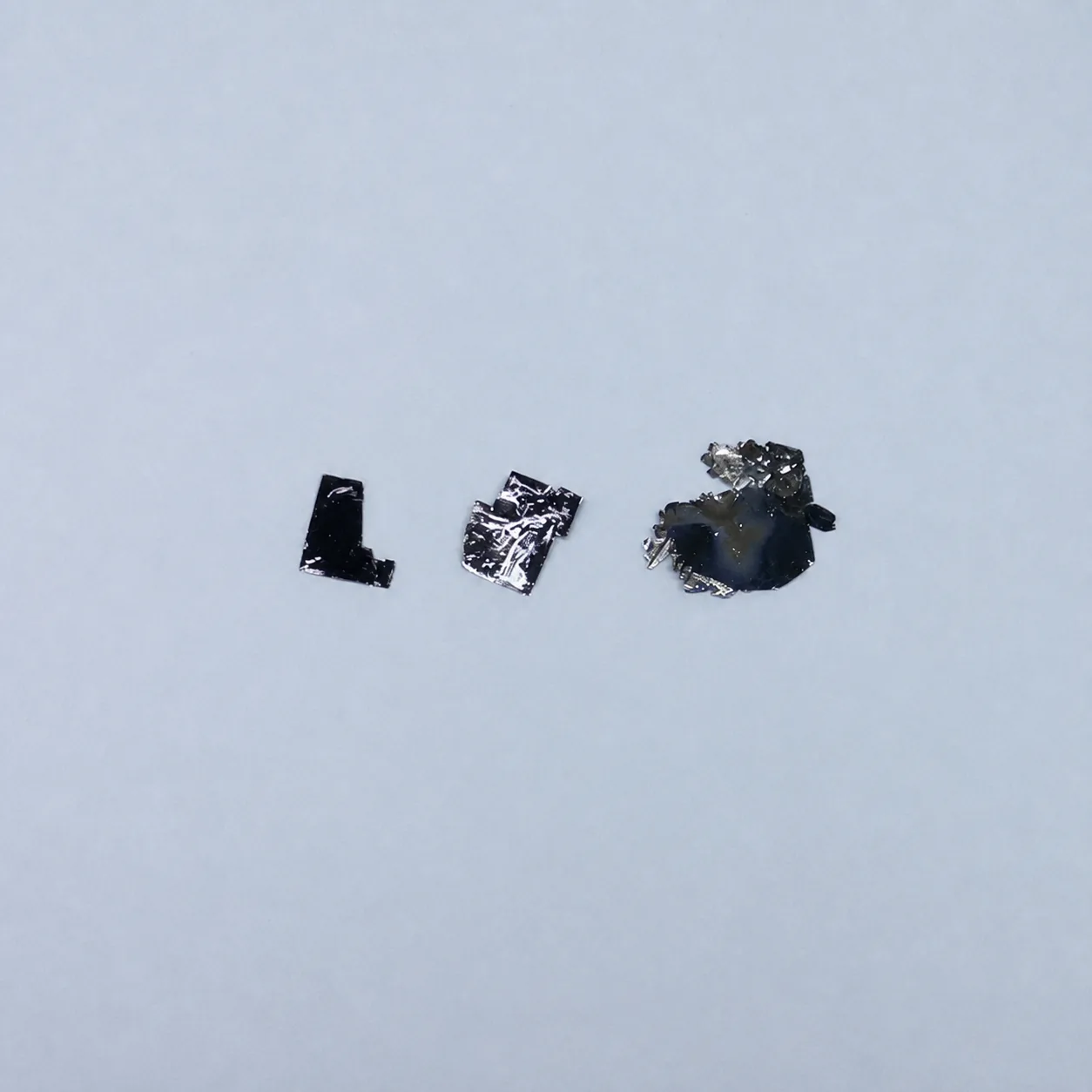
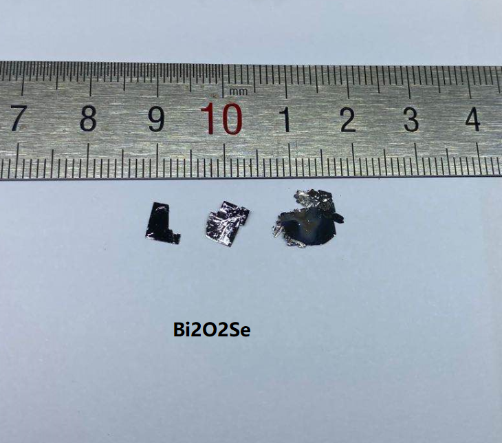
Bi₂O₂Se Crystals
Bi₂O₂Se is a layered semiconductor material with a unique structure combining a bismuth oxide layer and a selenium layer. It exhibits high electron mobility, strong anisotropic properties, and high thermal behavior, making it applicable to applications in optoelectronics, thermoelectrics, and 2D material research.
Sample Size Options:
Crystals larger than 10 mm²
Crystals larger than 25 mm²
Crystals larger than 100 mm²
Material Properties:
Layered Structure: Facilitates exfoliation into monolayers or few-layer sheets for specialized research.
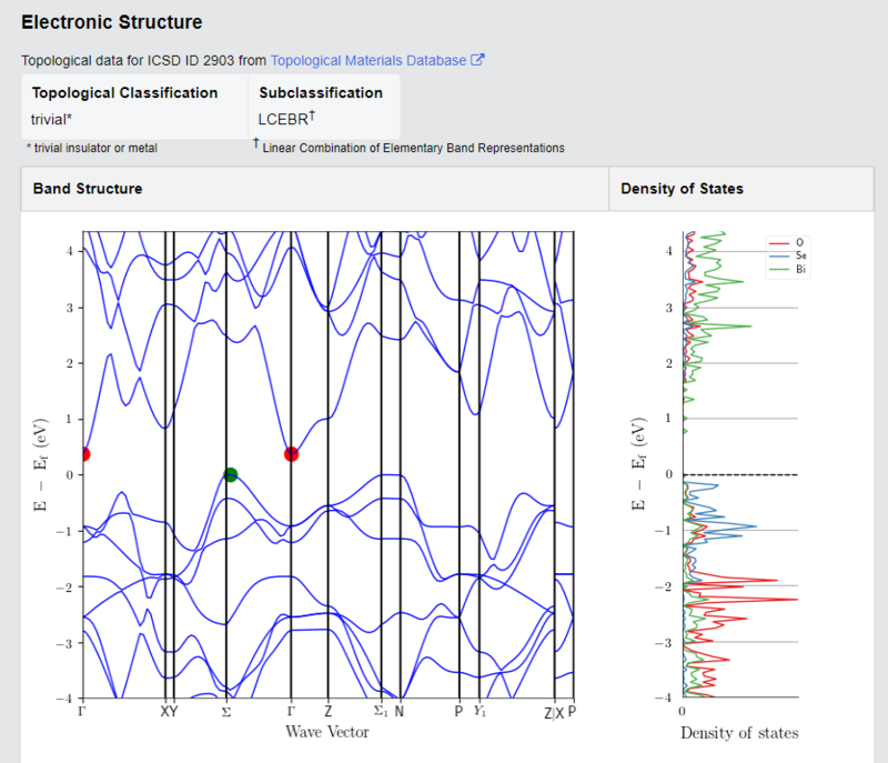
High Electron Mobility: Exhibits mobility above 450 cm²/V-s at room temperature. Wide Bandgap (~0.8 eV): Applicable to electronic and optoelectronic applications.
Environmental behavior: Maintains properties under ambient conditions.
Crystal Structure:
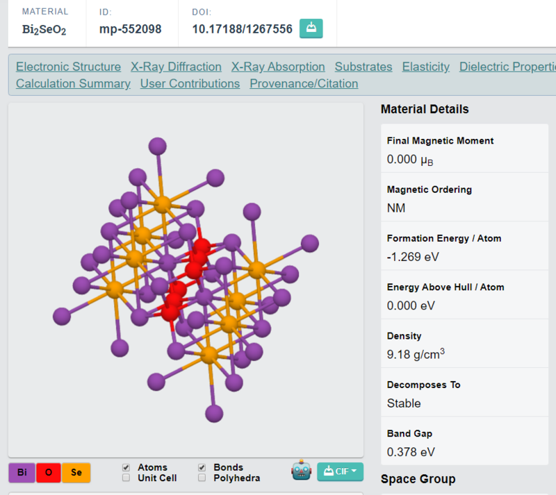
Type: Layered orthorhombic structure
Features: Combines oxide and chalcogenide layers for enhanced functionality.
Degree of Exfoliation:
Ease of Use: Readily exfoliates into thin layers for 2D material studies and specialized device applications.
Other Characteristics: Thermoelectric
Applications: High potential for waste heat recovery and energy harvesting.
Optoelectronic Potential: Applicable for photodetectors, light-emitting devices, and photonic applications.
Quantum Research Opportunities: Promising for studying anisotropic transport and electronic properties.
Applications:
Optoelectronics:
Applicable for photodetectors, infrared sensors, and photovoltaic devices. Quantum Materials Research:
Permits exploration of anisotropic electronic transport and quantum effects. Thermoelectric Devices:
Applicable to energy harvesting and waste heat recovery systems.
2D Material Studies:
Applicable for exfoliation into monolayers and assembly into van der Waals heterostructures. Energy
Applications:
Promising for energy conversion and catalytic processes.
| Option 1 | > 10 mm², > 100 mm², > 25 mm² |
|---|
Related products
-
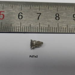
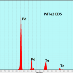
PdTe₂ Crystals
$696.09 -
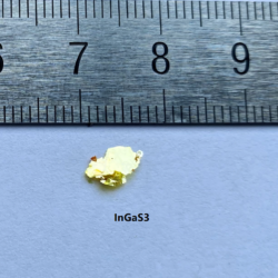
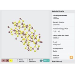
InGaS₃ Crystals
$696.09 -
WSeTe Crystals
Price range: $835.32 through $1,252.98 -
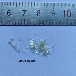
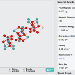
α-MoO₃ Crystals
Price range: $640.41 through $696.09 -
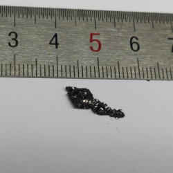
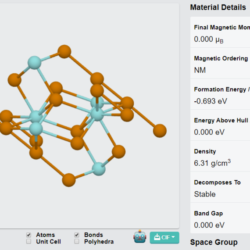
ZrTe₃ Crystals
Price range: $696.09 through $835.32 -
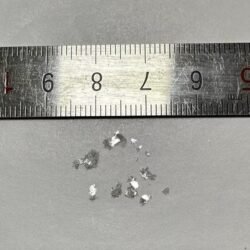
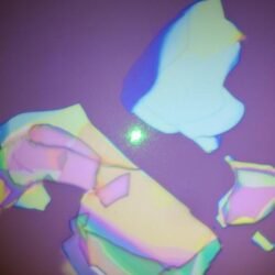
BiOCl Crystals
Price range: $696.09 through $793.55 -
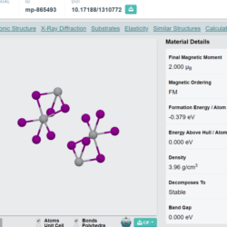
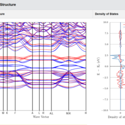
VI₃ Crystals
Price range: $696.09 through $835.32 -
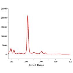
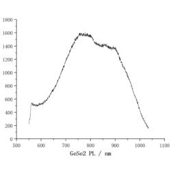
GeSe₂ Crystals
Price range: $696.09 through $793.55 -
FeBr₃ Crystals
Price range: $654.33 through $696.09 -
NiI₃ Crystals
Price range: $696.09 through $1,252.98