Showing 177–192 of 208 results
-
zł56.92
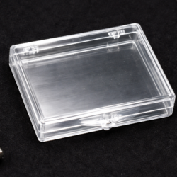
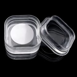
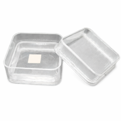
SP Series Sample Storage Boxes Application: For packaging, storage, and display of various optoelectronic components and general products. The design allows for logistics and transportation. Note: For highly sensitive, fragile, or precision devices that require suspension or immobilization, we recommend using Gel Boxes or Membrane Boxes instead. Detailed Specifications (Inner vs. Outer Dimensions): Model: SP-5510…
-
zł688.83 – zł2,429.17Price range: zł688.83 through zł2,429.17
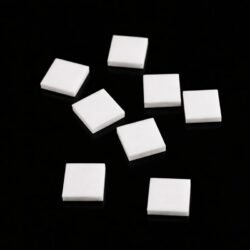
Square Alumina (Al₂O₃) Ceramic Substrates Overview: polycrystalline aluminum oxide (Al₂O₃) ceramic substrates in square and rectangular formats, intended for electrical insulation, thermal management, and laboratory research applications. Available in sizes from 5 × 5 mm up to 40 × 40 mm with multiple thickness options. Specifications: – Format: Square / Rectangular – Purity: ≥99.5% Al₂O₃…
-
zł119.08 – zł378.06Price range: zł119.08 through zł378.06
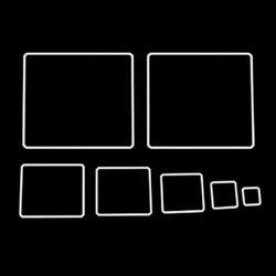
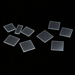
Square Sapphire (Al₂O₃) Single Crystal Substrates, C-Plane (0001) Overview: Single-crystal sapphire (Al₂O₃) substrates in square format, C-plane (0001) orientation. Available from 5 × 5 mm up to 50 × 50 mm, in 0.5, 1.0, 2.0, and 3.0 mm thickness, with single-side (SSP) or double-side (DSP) polishing. Applications include mask alignment, corner-referenced deposition, and lateral thin-film…
-
zł492.01 – zł1,175.71Price range: zł492.01 through zł1,175.71
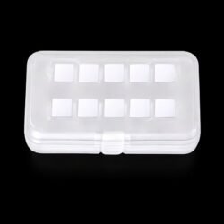
Standard Format: Square/rectangular substrates — 5 × 5 × 0.5 mm, 10 × 10 × 0.5 mm (other sizes on request). Polish: Single-Side Polished (SSP) or Double-Side Polished (DSP). Product Description: Overview: Strontium Titanate (SrTiO₃) single crystal substrates for high-temperature superconductivity (HTS), magnetron sputtering, and pulsed laser deposition (PLD). These cubic perovskite crystals are used…
-
zł1,797.26 – zł1,859.41Price range: zł1,797.26 through zł1,859.41
Standard Format: Circular wafer — 1″ diameter (25.4 mm) × 0.5 mm. Polish: Single-Side Polished (SSP) or Double-Side Polished (DSP). Product Description: Overview: Strontium Titanate (SrTiO₃) single crystal wafers for high-temperature superconductivity (HTS), magnetron sputtering, and pulsed laser deposition (PLD). These cubic perovskite crystals are used for the epitaxial growth of complex oxide thin films….
-
zł554.16 – zł3,537.60Price range: zł554.16 through zł3,537.60
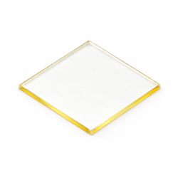
Standard LiF Optical Window for UV and IR Applications Product Overview: Lithium Fluoride (LiF) is a cubic crystal with optical transmission properties, especially in the vacuum ultraviolet (VUV) region. It has the lowest refractive index of all common infrared materials and is used in UV transmission windows, lenses, and prisms. Physical Properties: – Crystal Structure:…
-
zł657.75 – zł1,548.64Price range: zł657.75 through zł1,548.64
Strontium Lanthanum Aluminate (SrLaAlO₄) Single Crystal Substrate Physical Properties: – Crystal Structure: Tetragonal System – Lattice Constants: a=3.756Angstrom , c=12.636Angstrom – Melting Point: 1650 °C – Density: 5.92 g/cm³ – Hardness: 6~6.5 (Mohs) – Growth Method: CZ Standard Specifications: 1. Orientation – (001) miscut < 0.3° (customizable < 0.1°) – (100) miscut < 0.3° (customizable…
-
zł2,232.34 – zł2,688.15Price range: zł2,232.34 through zł2,688.15
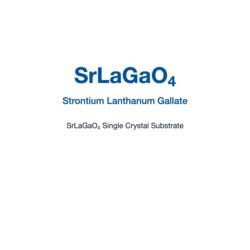
Strontium Lanthanum Gallate (SrLaGaO₄) Single Crystal Substrate Physical Properties: – Crystal Structure: Tetragonal System – Lattice Constants: a=3.843Angstrom , c=12.680Angstrom – Melting Point: 1500 °C – Density: 6.389 g/cm³ – Growth Method: Czochralski (CZ) Standard Specifications: 1. Orientation – (001) miscut < 0.3° – (100) miscut < 0.3° 2. Edge Orientation – Available 3. Surface…
-
zł419.49 – zł668.11Price range: zł419.49 through zł668.11
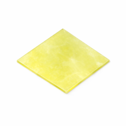
Tellurium Dioxide (TeO₂) Single Crystal Substrate Physical Properties: Crystal Structure: Tetragonal System Lattice Constants: a=b=4.81 Angstrom, c=7.613 Angstrom Density: 5.99 g/cm³ Melting Point: 733°C Mohs Hardness: 4 Mohs Growth Method: CZ Standard Specifications: Orientation: (110) miscut < 0.5 deg Edge Orientation: request
-
zł1,797.26 – zł2,418.81Price range: zł1,797.26 through zł2,418.81
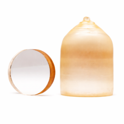
Terbium Gallium Garnet (TGG / Tb₃Ga₅O₁₂) Single Crystal Substrate Physical Properties: Crystal Structure: Cubic System Lattice Constant: a=12.355 Angstrom Density: 7.13 g/cm³ Mohs Hardness: 8 Mohs Melting Point: 1725°C Transmittance Range: 400 ~ 1100 nm Verdet Constant: 40 rad/T/m @1064nm Growth Method: CZ Standard Specifications: Orientation: (111) miscut < 0.3 deg Edge Orientation: Available
-
zł1,548.64 – zł3,102.51Price range: zł1,548.64 through zł3,102.51
Terbium Scandate (TbScO₃) Single Crystal Substrate Physical Properties: – Crystal Structure: Orthorhombic System – Lattice Constants: a=5.4543 Angstrom, b=5.7233 Angstrom, c=7.9147 Angstrom – Density: 6.6 g/cm³ – Melting Point: 2127 °C – Growth Method: CZ Standard Specifications: 1. Orientation – (110) miscut < 0.3° – (001) miscut < 0.3° – (100) miscut < 0.3° –…
-
zł305.54 – zł1,362.18Price range: zł305.54 through zł1,362.18
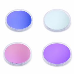
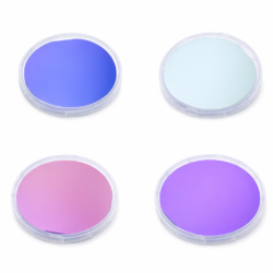
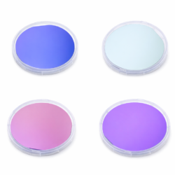
Thermal SiO₂ on N-Type (Arsenic-Doped) Si (100) Wafers Overview Our thermal silicon dioxide (SiO₂) wafers are fabricated using high-temperature thermal oxidation on heavily doped N-type (arsenic-doped) Si (100) substrates with ultra-low resistivity of 0.001–0.005 Ω·cm. The highly doped silicon substrate has high electrical conductivity, while the thermally grown SiO₂ layer has consistent film density, high…
-
zł305.54 – zł1,362.18Price range: zł305.54 through zł1,362.18
Thermal SiO₂ on N-Type (Phosphorus-Doped) Si (100) Wafers Overview Our thermal silicon dioxide (SiO₂) wafers are fabricated using high-temperature thermal oxidation on N-type (phosphorus-doped) Si (100) substrates with a resistivity range of 1–10 Ω·cm. Thermally grown oxide has consistent film density, high thickness uniformity, low interface trap density, and high dielectric strength compared to deposited…
-
zł305.54 – zł1,362.18Price range: zł305.54 through zł1,362.18
Thermal SiO₂ on P-Type (Boron-Doped) Si (100) Wafers Overview Our thermal silicon dioxide (SiO₂) wafers are fabricated using high-temperature thermal oxidation on P-type (boron-doped) Si (100) substrates. Available resistivity ranges include 1–10 Ω·cm and heavily doped 0.001–0.005 Ω·cm options. Thermally grown SiO₂ has consistent film density, high dielectric strength, and a consistent Si/SiO₂ interface compared…
-
zł305.54 – zł1,300.02Price range: zł305.54 through zł1,300.02
Thermal SiO₂ on Undoped Si (100) Wafers Overview Our thermal silicon dioxide (SiO₂) wafers are fabricated using high-temperature dry/wet thermal oxidation on undoped Si (100) substrates. Thermal oxide has consistent film density, high uniformity, low defect density, and consistent electrical insulation compared to deposited oxide films. These wafers are used in semiconductor research, MOS structure…
-
zł398.78 – zł2,170.19Price range: zł398.78 through zł2,170.19
Product Name: TiO₂ (Titanium Dioxide) Single Crystal Substrates (Rutile Phase) Packaging & Variant Options: – Packaging: 100-class clean bag, 1000-class clean room – Available Dimensions (Square/Rectangular): – 5 × 3mm,5 × 5mm, 10 × 5mm, 10 × 10mm, 15 × 15mm, 20 × 20mm – Available Dimensions (Circular): – Φ10mm, Φ15mm, Φ20mm, Φ1″, Φ2″ –…