
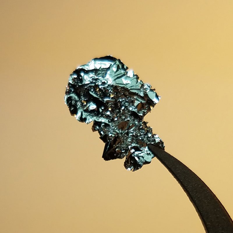
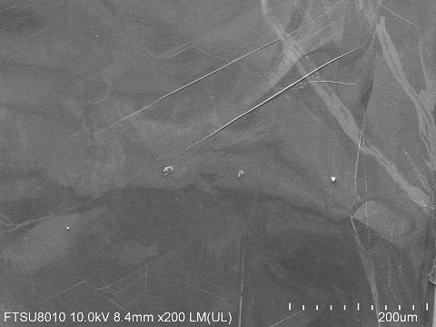
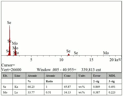
MoSe₂ Crystals
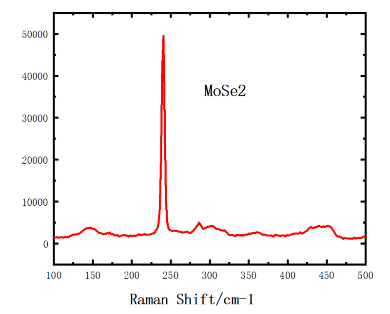
MoSe₂ (Molybdenum Diselenide) is a layered transition metal dichalcogenide (TMD) with a van der Waals structure. It exhibits a variable bandgap, spin-orbit coupling, and electronic and optoelectronic properties, supporting applications in nanoelectronics, optoelectronics, spintronics, and 2D material research. MoSe₂ crystals are synthesized using the Chemical Vapor Transport (CVT) method.
Sample Size Options:
Crystals larger than 10 mm²
Crystals larger than 25 mm²
Crystals larger than 100 mm²
Material Properties:
Layered van der Waals Structure: Permits exfoliation into monolayers or few-layer nanosheets for 2D material studies.
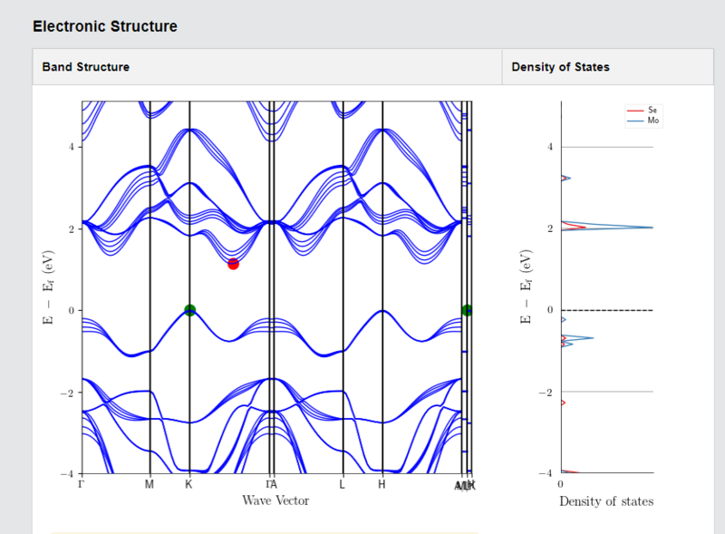
Variable Bandgap: Exhibits an indirect bandgap (~1.1 eV) in bulk and a direct bandgap (~1.55 eV) in monolayer form, applicable to optoelectronic applications.
Carrier Mobility: Applicable for transistors, field-effect devices, and nanoelectronics.
Photoluminescence: Monolayer MoSe₂ exhibits intense photoluminescence, supporting light-emitting-device research. Spin-Orbit Coupling: Permits spintronic applications and valleytronic effects in quantum materials research.
Crystal Structure:
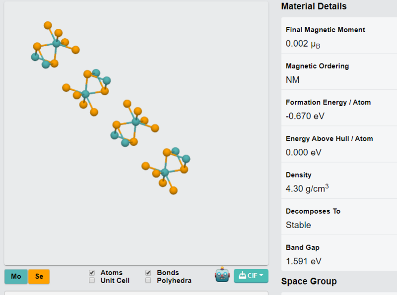
Type: Hexagonal (2H phase) layered structure
Features: Layers applicable for thin-film fabrication and nanoscale device applications.
Degree of Exfoliation:
Ease of Use: Exfoliated into monolayers or few-layer nanosheets for materials research and heterostructure assembly.
Other Characteristics:
Quantum Confinement Effects: Exhibits excitonic effects and light-matter interactions in monolayer form.
Optical Absorption: Visible- and infrared-spectrum absorption, applicable to photodetectors and solar cells.
Applications:
Optoelectronics:
Applicable for photodetectors, LEDs, and photovoltaic cells due to light absorption and photoluminescence. Nanoelectronics:
Used for transistors, memory devices, and flexible electronic circuits. Spintronics & Quantum Computing:
Permits research on spin-orbit coupling, valley polarization, and quantum technologies.
2D Material Studies:
Applicable for exfoliation into monolayers and assembly into van der Waals heterostructures. Sensors & Catalysis:
Used for gas detection, chemical sensing, and electrocatalytic applications such as hydrogen evolution reactions (HER). Synthesis Method:
Chemical Vapor Transport (CVT).
| オプション1 | > 10 mm², > 100 mm², > 25 mm² |
|---|
関連商品
-
VS₂ Crystals
価格帯: ¥111,155 – ¥126,717 -
WSeTe Crystals
価格帯: ¥133,386 – ¥200,081 -
WSSe Crystals
価格帯: ¥133,386 – ¥200,081 -
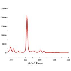
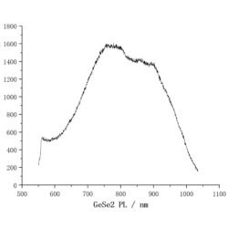
GeSe₂ Crystals
価格帯: ¥111,155 – ¥126,717 -
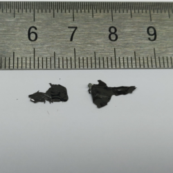
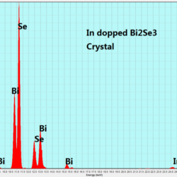
InBiSe₃ Crystals
価格帯: ¥111,155 – ¥200,081 -
NiI₃ Crystals
価格帯: ¥111,155 – ¥200,081 -
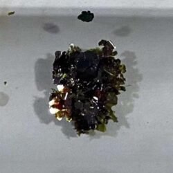
CrBr₃ Crystals
¥111,155 -
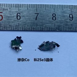
Co-Doped Bi₂Se₃ Crystals
¥111,155 -

FeCl₃ Crystals
価格帯: ¥111,155 – ¥200,081 -
FeBr₃ Crystals
価格帯: ¥104,486 – ¥111,155