
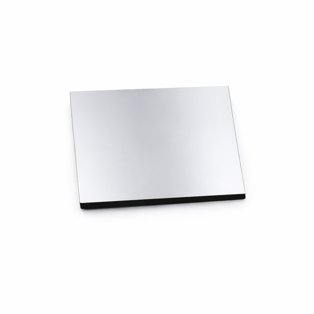
Silicon (Si) Single Crystal Substrates (N-type, doped), 10 pcs/pack
Price range: $132.25 through $215.78
Silicon (Si) Single Crystal Substrates (Wafers)
Physical Properties:
– Crystal Structure: Cubic System
– Lattice Constant: a=5.4301 Angstrom
– Hardness: 6.5 (Mohs)
– Density: 2.329 g/cm³
– Melting Point: 1414 °C
– Growth Method: CZ and FZ
Standard Specifications:
1. Orientation Note
– Other orientations customizable
2. Surface Quality
– Polish: Single-side polished / Double-side polished
Silicon Wafer Grade Selection Guide
We has two primary wafer grades for research and semiconductor applications: Research Grade and Prime Grade (Device Grade). Each grade is specified for different experimental and fabrication needs.
Research Grade Silicon Wafers
(Also known as: Lab Grade / General Research Grade)
Description:
Research-grade silicon wafers are quality polished wafers designed for academic research, material science, thin film deposition, and general laboratory use. They has high surface quality and flatness applicable to most non-device fabrication experiments.
Key Characteristics:
* Quality single crystal silicon
* Single-side or double-side polished
* Good surface flatness and cleanliness
* Cost-functional for routine research
* Minor surface defects or particles may be present (non-device-critical)
* Not certified for integrated circuit fabrication
Recommended Applications
* Thin film deposition (Au, Pt, Ti, Al, etc.)
* 2D materials growth and transfer
* Optical and photonic experiments
* Surface chemistry and catalysis
* SEM/AFM characterization
* Electrochemistry substrates
* General university research
Standard For:
Most academic and R&D laboratory use
—
Prime Grade Silicon Wafers (Device Grade)
(Semiconductor / IC / Device Fabrication Grade)
Description:
Prime-grade silicon wafers represent semiconductor industry device-grade quality. These wafers feature ultra-low surface roughness, extremely low defect density, and tightly controlled electrical and crystallographic specifications. Applicable to microfabrication, MEMS, and semiconductor device production.
Key Characteristics:
* Semiconductor device fabrication grade
* Ultra-low particle and defect density
* High surface roughness (typically <0.5 nm Ra)
* Tight resistivity and orientation tolerance
* High uniformity across wafer
* Cleanroom-fits packaging
* Applicable to photolithography and microfabrication
Recommended Applications:
* Micro/nano device fabrication
* MEMS processing
* Photolithography
* Semiconductor device research
* Epitaxy and thin-film growth requiring ultra-clean surfaces
* MOS/MIS structure fabrication
* Specialized university cleanroom use
Standard For:
Device fabrication and high-precision semiconductor research
—
How to Choose the Right Grade:
Application Type | Recommended Grade
Thin film deposition | Research Grade
Catalysis / materials research | Research Grade
2D materials / graphene transfer | Research Grade
Optical experiments | Research Grade
SEM/AFM substrates | Research Grade
Teaching labs | Research Grade
Photolithography | Prime Grade
MEMS fabrication | Prime Grade
Semiconductor devices | Prime Grade
Epitaxy growth | Prime Grade
Cleanroom fabrication | Prime Grade
—
Quick Recommendation:
For 90% of university and lab research: Research Grade is sufficient
For device fabrication or cleanroom processing: Choose Prime Grade
| Option 1 | 10 × 10 × 0.5 mm, Double-side Polished, Research Grade, 10 × 10 × 0.5 mm, Single-side Polished, Research Grade, 20 × 20 × 0.5 mm, Double-side Polished, Research Grade, 20 × 20 × 0.5 mm, Single-side Polished, Research Grade, 5 × 5 × 0.5 mm, Double-side Polished, Research Grade, 5 × 5 × 0.5 mm, Single-side Polished, Research Grade |
|---|---|
| Option 3 | N-type (As-doped), N-type (Ph-doped), N-type (Sb-doped) |
| Orientation | (100), (110), (111) |
Related products
-
Silicon (Si) Single Crystal Wafers (P-type, doped)
Price range: $48.71 through $224.13 -
Silicon (Si) Single Crystal Substrates (P-type, doped), 5 pcs/pack
Price range: $132.25 through $215.78 -
Silicon (Si) Single Crystal Substrates (Undoped), 10 pcs/pack
Price range: $132.25 through $215.78 -
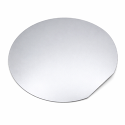
Silicon (Si) Single Crystal Wafers (Undoped)
Price range: $48.71 through $265.90 -
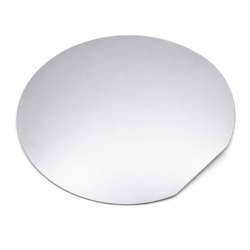
Silicon (Si) Single Crystal Wafers (N-type, doped)
Price range: $48.71 through $265.90